Blog & Design Guide

Combining several PCB designs on one panel can simplify handling, but it creates one manufacturing release with several board identities. Before choosing a multi design PCB panelization plan, confirm common construction and process, then define how each child design will be identified, tested and revised.
This article covers bare-board panel planning. Mixed panels are not always suitable; the decision depends on the designs, manufacturing route and delivery plan.
In this article
Treat a mixed panel as a parent release that maps to several child boards. Before checking whether the designs can share a process, make sure the drawing and manifest identify:
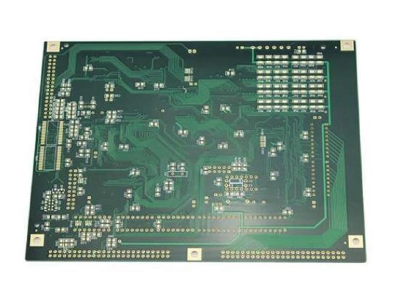
The panel image shows three visually distinct board sections, but appearance alone does not prove that they are separate product IDs or revisions. 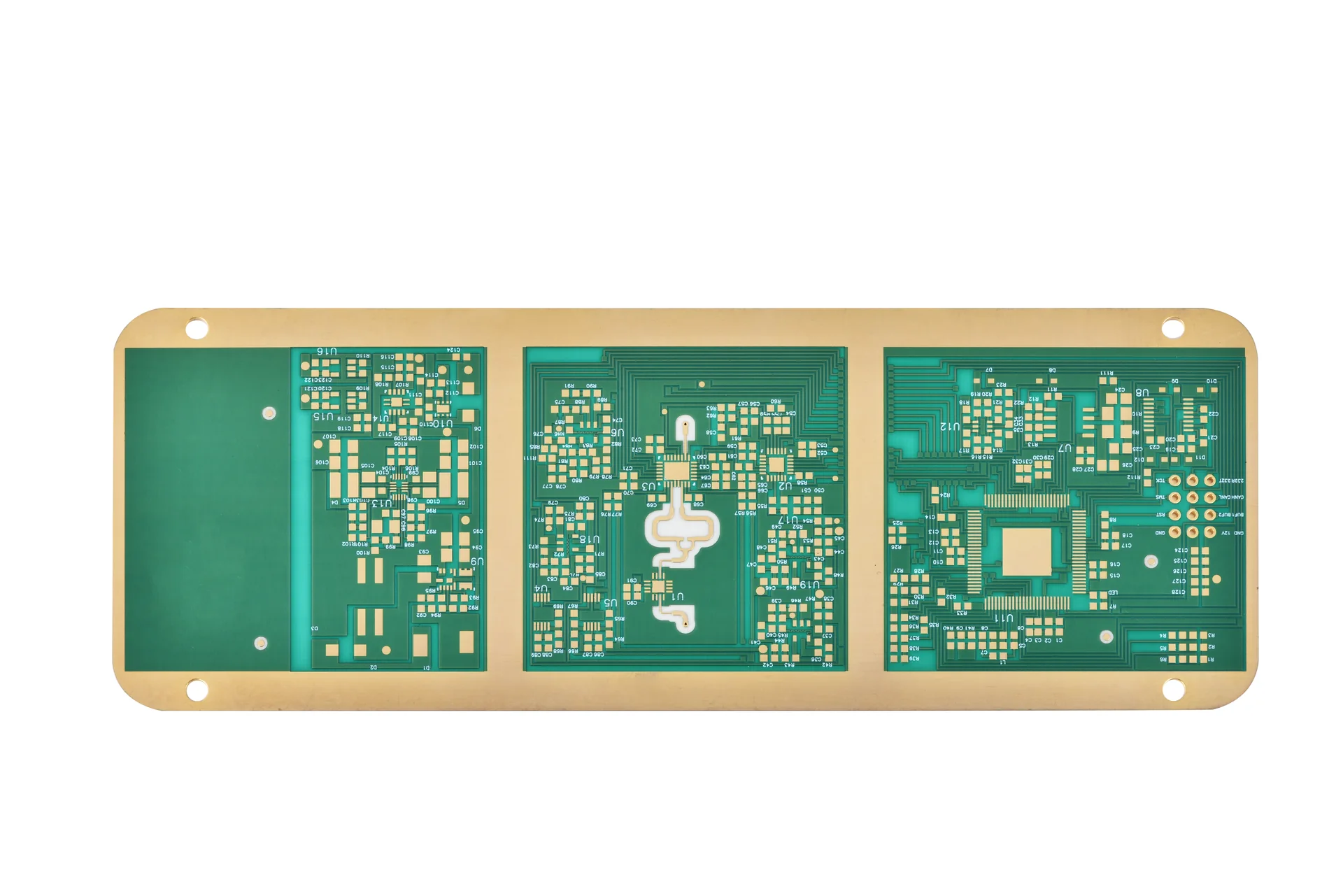
The image shows three visually distinct board sections; the approved panel map defines product identity and revision.
Start with the reason for combining boards. A mixed panel may suit small designs that share one construction and must travel together. If one board needs a different material, finish, stack-up or acceptance route, the combination may add review or handling rather than simplify it.
Compare the candidate designs before creating the panel drawing:
| Question | A combined panel may fit when | Keep designs separate when |
|---|---|---|
| Construction | The boards share material, layer construction and finish requirements. | A board needs a different stack-up, base material, copper or finish route. |
| Revision state | Each board revision is approved and can be frozen in one panel release. | One design is still changing or has unresolved requirements. |
| Acceptance | The same lot-level acceptance and record plan can identify each board. | Different board requirements would be obscured by one shared acceptance basis. |
| Delivery | The pieces can be delivered, labeled and tracked as one planned group. | Different destinations, quantities or release dates require separate control. |
Ask the fabricator to review a proposed combination before freezing the panel. The supplier may prefer to build some pieces separately or recommend a different layout. That response should be recorded as a manufacturing decision, not treated as a design change made without approval.
Check construction before comparing empty space. Review each stack-up, material, copper requirement, finish and controlled process note. Confirm that one agreed manufacturing route can meet every board requirement.
Check how each design will be placed and separated. Irregular outlines, edge copper, holes or sensitive pads can affect tabs, scoring or routing. No single spacing or edge clearance suits every design and machine. Put proposed values on the drawing and ask the supplier to confirm them.
Review the layout for overlapping outlines and make the panel boundary clear. Check that rails, tooling holes and fiducials stay outside each child board’s controlled area. If the supplier changes the geometry, update the panel drawing and revision; do not use a preview image as the only release record.
Do not collapse several products into one anonymous “panel” file. Give the panel its own ID and revision, then list each child board’s ID, revision and quantity. Keep a separate record of the manufacturing data used for each design.
A release manifest can use a compact structure such as:
IPC-2581 is one data-exchange format for printed-board manufacturing information. Its structure includes a history record, but does not provide a customer’s complete revision-control workflow. Keep the panel release linked to approved child data and retain the approval trail in the project records.
For a practical review, KnownPCB’s high-mix, low-volume workflow discusses revision-aware builds and variant control. The buyer should still identify the exact child designs and panel revision in the order package.
The panel drawing should show the outside boundary, each child outline, orientation, board count, rails, tooling holes and required fiducials. Mark the separation method, such as scoring or routed breakaway tabs, and any edge or copper condition that needs review.
Label panel-only elements clearly. A rail, breakaway tab or fiducial may support handling or alignment, but it should not be mistaken for a finished-board requirement in later revisions.
State whether boards should arrive attached or as individual pieces, what edge condition is acceptable, and how parts should be protected and labeled. If several board IDs share a shipment, define how they will stay separate. Explain what “cleanly depanelize” means in the drawing or acceptance note.
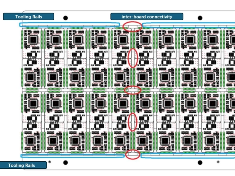
A repeated design is different from a mixed panel. This image shows one design repeated across an array and is included for comparison. 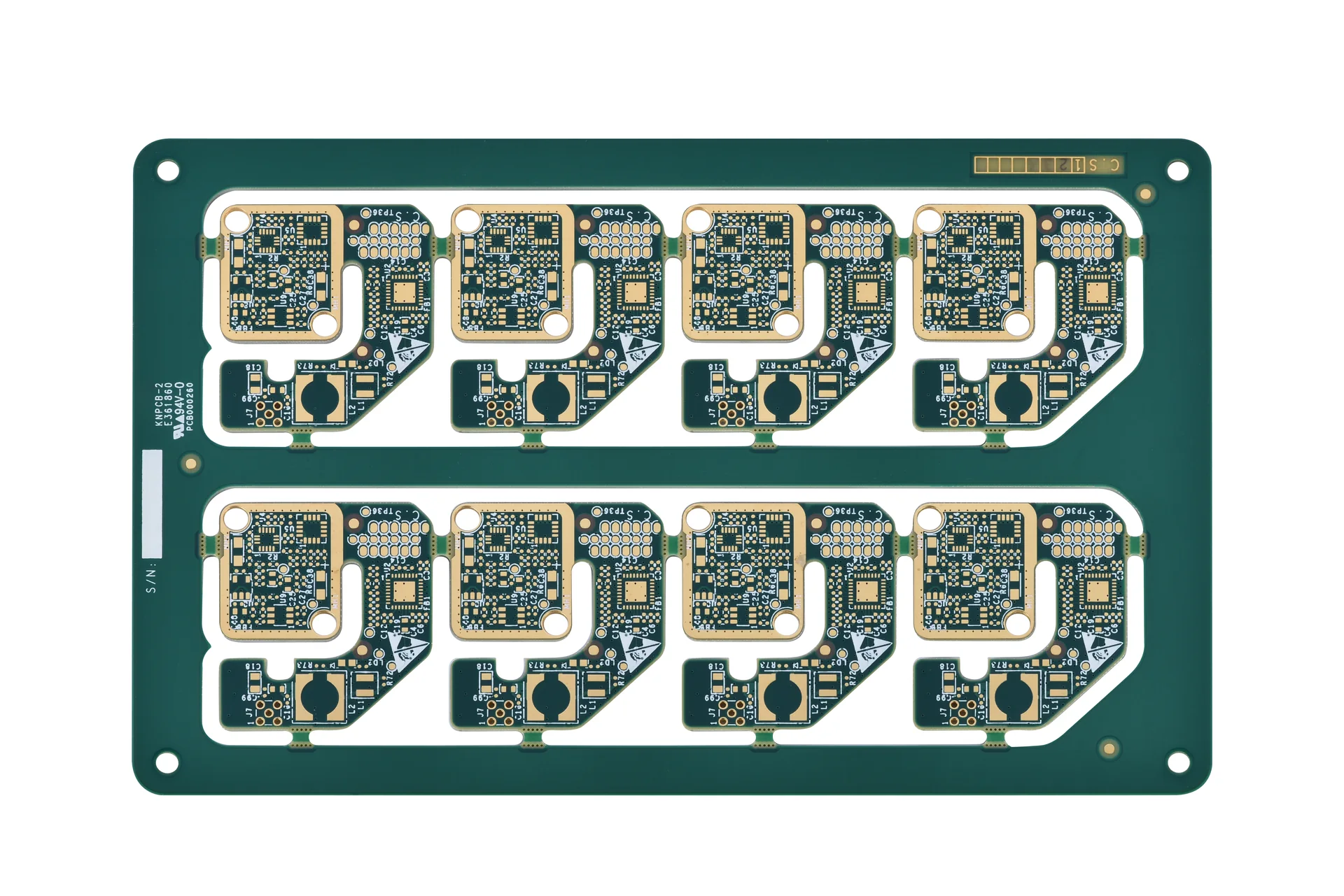
A repeated array uses one design in multiple positions; a mixed panel contains separately identified designs.
Define how inspection results link to the panel and child designs. Ask which electrical or dimensional tests apply, how board positions are identified, and how a report distinguishes a failing child. There is no universal disposition for a single failed piece; state whether the panel is held, boards can be separated, or another response applies.
Keep traceability at the level needed for release. If a report identifies only the panel, it may not show which child board passed. Use a board marking, packing label or agreed record to link each piece to the panel map.
When a child design changes, review the effect on geometry, separation, material compatibility, tests and quantities. Increment the panel revision when its contents or arrangement change. Make sure the data and order point to the same parent and child revisions.
Review the package with the manufacturer and each design owner. KnownPCB’s quality management overview provides context on inspection and documentation. For a mixed-panel question, contact KnownPCB with the drawing and controlled child data.
Configuration management guidance from NASA describes baselines, change evaluation and verification. It is not a PCB standard, but its general sequence applies: identify the released panel configuration, approve changes, issue them to the manufacturer and verify the lot against the approved data.
Yes. Record the identity and revision of each child board as well as the panel’s own ID and revision. A parent panel drawing does not replace the source records for its individual designs.
Define the disposition before ordering. The required response may depend on test coverage, customer risk and whether individual pieces can be separated and identified. Do not assume the supplier’s default process matches the buyer’s lot-acceptance rules.
IPC-2581C’s scope describes a structured data format for printed-board tooling, manufacturing, assembly and inspection information. NASA-HDBK-1004 provides general engineering guidance on configuration baselines and change verification, not PCB panel acceptance criteria.
Proven by 7 industries, 4000+ customer projects
Please contact us at sales@knownpcb.com, ask for engineering support here or use the form below to reach out to KnownPCB | Request a Manufacturing QuoteInclude your quantity, target delivery date and key requirements. File handling and NDA information. |