
“Double sided metal core PCB” is an incomplete construction note. A buyer may mean two copper circuit layers above one metal base, or circuits on opposite faces of a metal core. Those arrangements have different heat paths, different access for components, and different requirements around holes.
The cross-section resolves the ambiguity. Draw every copper layer, dielectric layer, and metal element in order, then show how a connection travels from one circuit layer to the other. The conductive metal must have an explicit electrical role. Leaving that role unstated creates a problem that neither a finished-board photograph nor a two-layer Gerber set can resolve.
Contents
In one construction, both circuit layers are located above a metal backing. The interlayer dielectric and the insulation to the backing are separate parts of the stack. The metal side may remain available for contact with a heatsink, while components and interconnections occupy the circuit side.
In another construction, the metal lies between circuits on opposite faces. Each face needs its own insulation from the core. If the two circuit faces must connect electrically, the connection crosses a conductive obstacle. The design therefore needs a manufacturing route that preserves insulation around the interconnect.
These are descriptions of possible architectures, not interchangeable catalogue items. Availability, material choices, minimum geometry, and processing sequence need confirmation for the proposed board. Do not rename a conventional double-sided FR-4 board with a separately attached metal heatsink as the same structure without showing the interface.
| Construction description | Where the metal sits | Question for the section drawing |
|---|---|---|
| Two circuits above metal backing | Below both circuit layers | How do the circuits connect without reaching the backing? |
| Circuits on opposite faces of metal | Between the circuit faces | How is each crossing insulated through the conductive core? |
| FR-4 circuit attached to a separate heatsink | Outside the PCB laminate | What electrical and thermal interface joins the two parts? |
The KnownPCB metal-core PCB construction page is the commercial starting point for that review. For the material trade-offs common to several constructions, refer to the existing metal-core PCB material-selection article. Keep the new drawing specific to where its metal sits and how each circuit is insulated.
The panel photograph below shows external circuit outlines and mounting holes. It cannot distinguish the possible internal architectures or establish the insulation surrounding a through-hole.
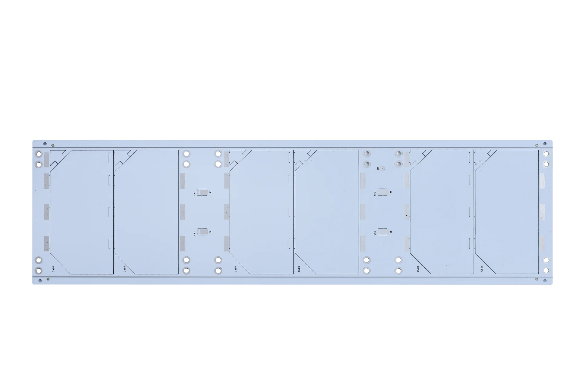
A surface photograph cannot establish the internal core position or the insulation around a plated hole.
A normal plated barrel is conductive. If it touches a metal core that is intended to remain separate from the circuit, the isolation is lost. Calling the hole PTH defines a plated connection but does not explain how that connection crosses the core safely.
One possible process uses a larger clearance in the metal, an insulating fill or sleeve, and a smaller finished hole formed within the insulated region. Other constructions use different sequences. The fabricator must specify the actual process, because the dimensions, registration budget, and acceptable defects depend on it.
The drawing should distinguish finished hole diameter from clearance in the metal. It should identify the intended insulation annulus, layer connections, and positional relationship to the core. A single drill diameter cannot carry all four meanings. Include the relevant section view alongside the drill table.
Check the tolerance combination rather than the nominal concentric drawing. Hole position, metal opening position, finished diameter, and insulation condition all affect the smallest remaining separation. Ask the fabricator to review this combination before reducing board area or placing several such holes close together.
An electrical netlist also needs an explicit core node when the construction makes the core accessible. If the core is floating, that condition still requires a documented verification plan. If it is bonded to chassis, identify the bonding feature and keep it separate from unintended circuit connections.
A screw through an unplated hole can connect a metal base to a housing even though the hole has no copper barrel. A washer can overlap a circuit pad. An exposed routed edge can become a contact surface. Evaluate the assembled mechanical stack, including any bush, spacer, washer, and interface pad.
Specify where exposed metal is permitted and where it must remain insulated. Show countersinks, counterbores, slots, and edge features in the mechanical drawing. A countersink changes the local distance to copper and can remove insulation that appeared adequate in a flat top view.
The back surface also has a function. If it is the primary heat-transfer surface, specify its contact region and finish according to the assembly design. Adding circuits to that surface may reduce the area available for contact or require an electrically insulating interface. That changes the thermal path and must be evaluated.
For this reason, a drawing review should include the mounting assembly or a section through the fastener. Reviewing only the electrical artwork leaves the metal hardware outside the decision, even though it can define the circuit-to-chassis connection in the finished product.
Henkel’s THERMAL CLAD selection document lists thermal and electrical material properties with their test methods. That information supports material selection, but it does not certify a fabricated hole, an exposed edge, or a complete hardware assembly. Match a datasheet value to its material grade and thickness before using it in a design review.
Define acceptance at the feature level. Useful questions include whether the circuit-to-core relationship is correct, whether a plated interconnect remains isolated along its passage, and whether the mounting hole and edge are free of unintended conductive bridges. The agreed inspection method must be able to find the defect being controlled.
Routine netlist testing and a specified dielectric-withstand evaluation establish different things. Do not substitute an ordinary open-and-short result for a high-voltage qualification. If the project requires an additional insulation evaluation, agree its method, responsibility, availability, and records before ordering; it is not assumed to be included.
The fixture photograph below illustrates bare-board electrical testing only. It does not demonstrate a particular test voltage or establish an insulation certification.
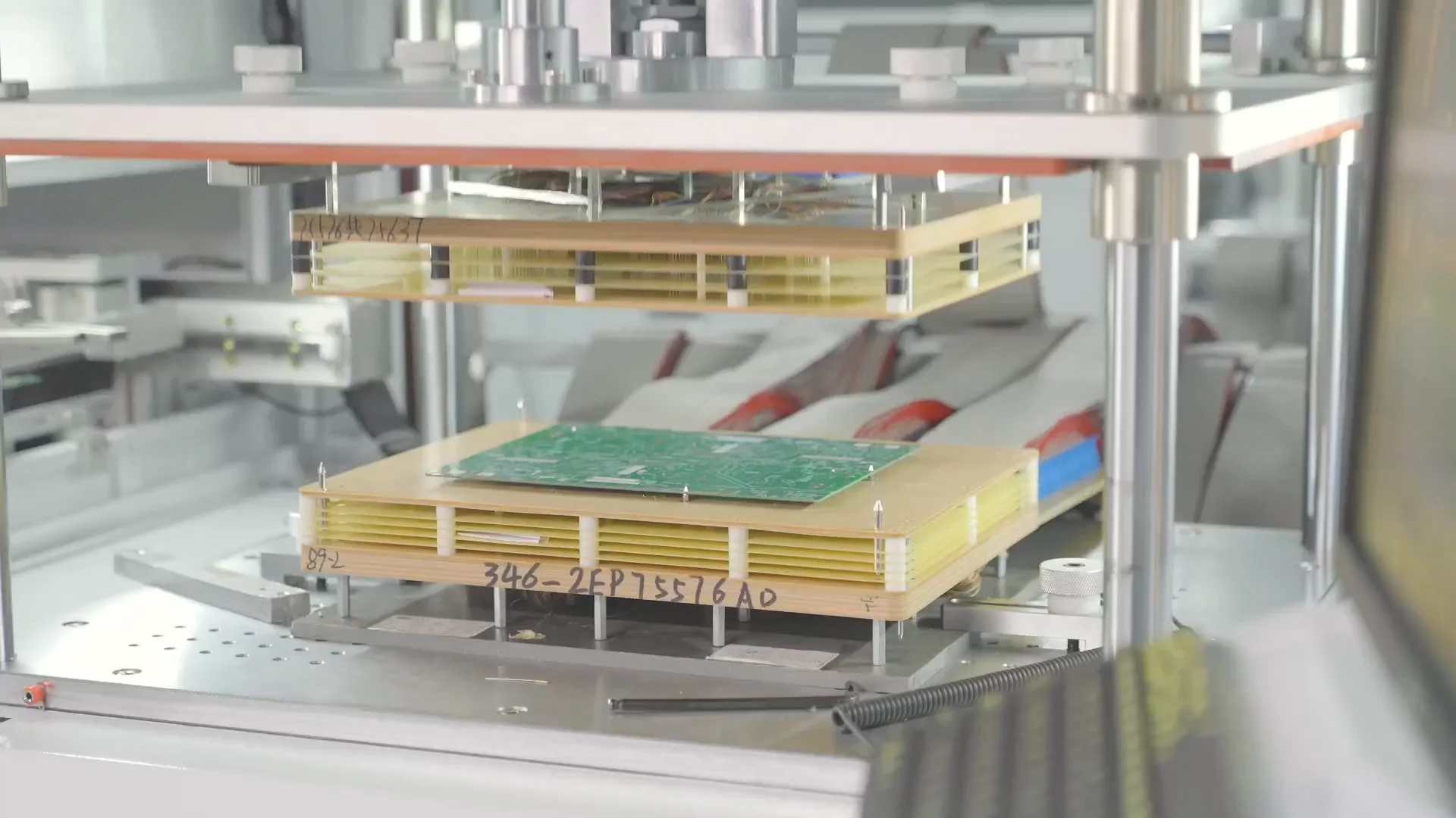
Bare-board electrical testing checks the agreed netlist; this image does not document a dielectric-withstand test.
The package needs a complete stackup, material designations, layer artwork, drill data, outline drawing, core-to-net definition, and section views of insulated interconnects. Mark which dimensions apply after processing and which belong to an intermediate metal opening. Identify controlled surfaces for heatsink contact.
Include approved substitution rules. A change in dielectric thickness or core material can alter electrical separation, heat flow, machining, and overall thickness at the same time. Keeping only the nominal board thickness fixed does not preserve the original design.
Before release, compare the supplier’s proposed cross-section with the electrical and mechanical files. Check the same hole identifiers in every document. Resolve differences in writing, especially where “double sided” is being used differently by the designer and the fabricator.
A double-sided metal-core PCB DFM enquiry should attach that cross-section and identify the features that need electrical isolation from metal. A defined construction lets the supplier answer the manufacturability question before choosing a drill route or quoting a board that solves a different problem.
March/20/2026Automotive Multi Camera System Demands and Challenges in PCB Process
May/15/2026MOSFETs and SMT Integration
April/23/2026Through-Hole Assembly Capabilities & DFM Checklist
May/27/2026DFM for PCB with Large-Footprint Components
July/10/2026Prototype PCB Assembly vs Low Volume PCB Assembly