
+86(755) 27944155 sales@knownpcb.com
Home October/01/2026
  1. 112G PAM4 PCB Design: Baud Rate and Channel Budgets
    112G PAM4 PCB Design: Baud Rate and Channel Budgets

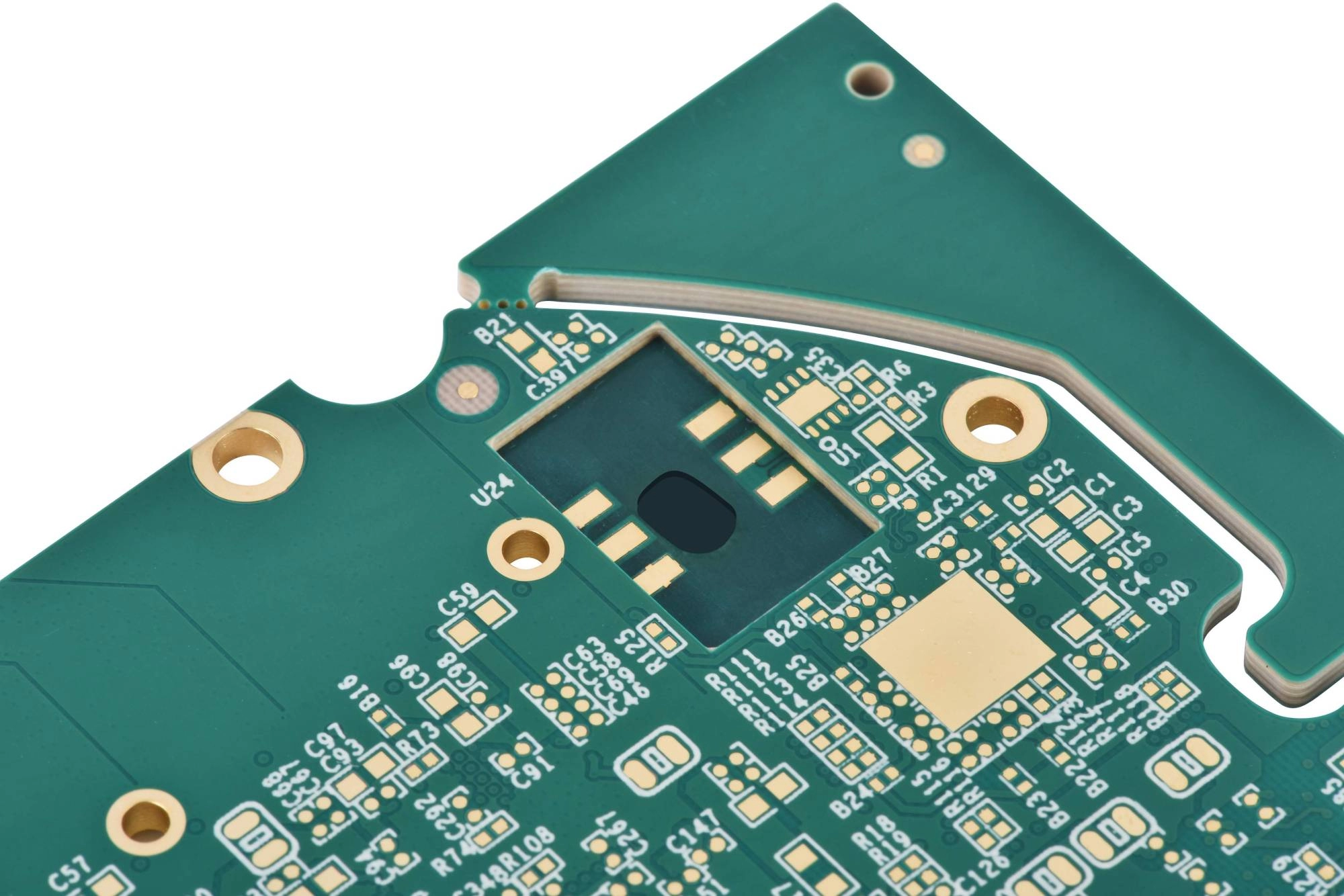
    112G PAM4 PCB design starts with a defined electrical channel, not a laminate label. The engineer needs the gross serial rate, the signaling format, and the reference planes used by the interface sp...
  2. Thermal Via Resistance: Plating, Diameter and Arrays
    Thermal Via Resistance: Plating, Diameter and Arrays

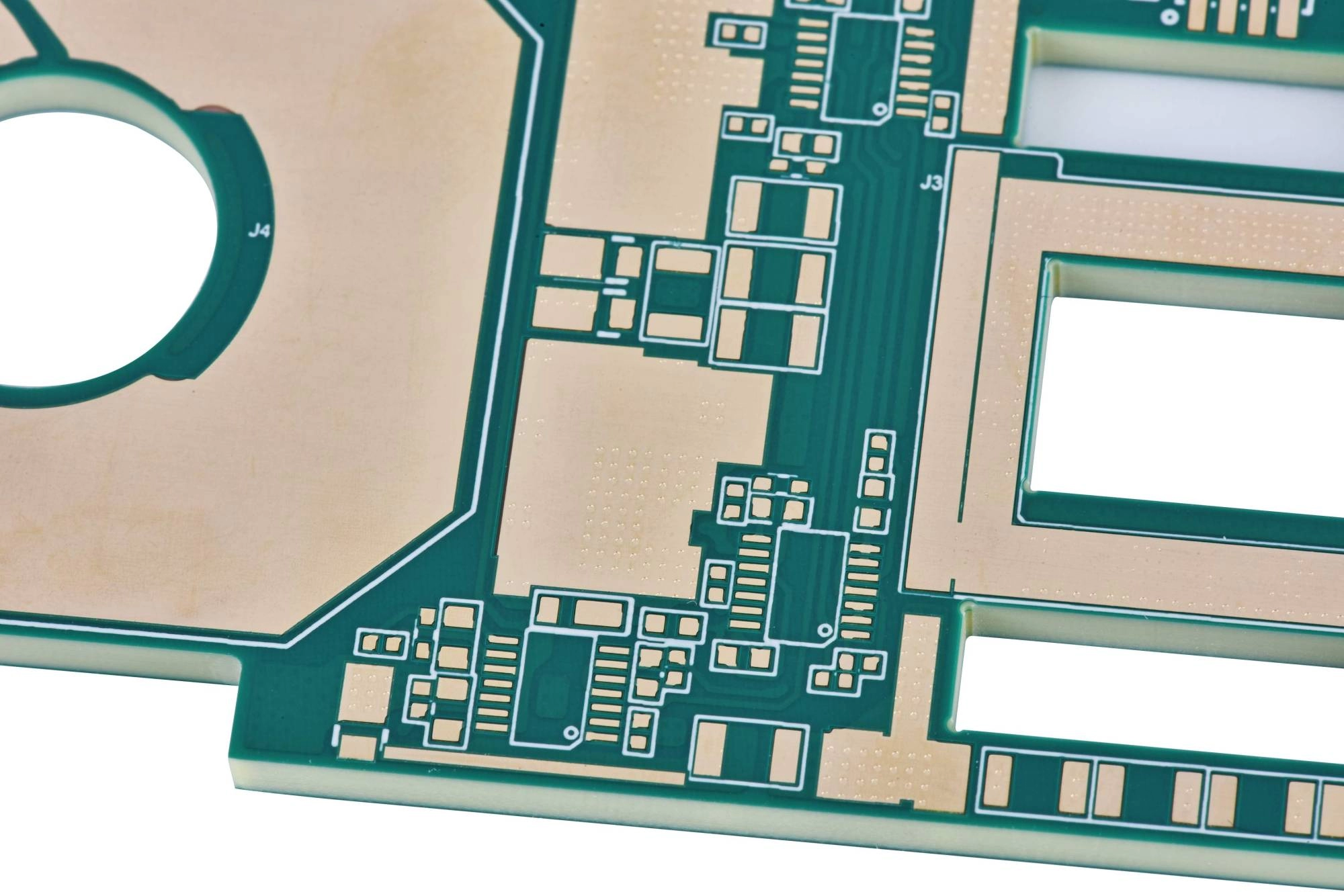
    Thermal via resistance can be estimated from the copper in the via barrel. The first calculation uses the copper cross-section, the board thickness, and an assumed copper conductivity. It gives an i...
  3. PCB Z-Axis Expansion: CTE, Tg and Via Barrel Strain
    PCB Z-Axis Expansion: CTE, Tg and Via Barrel Strain

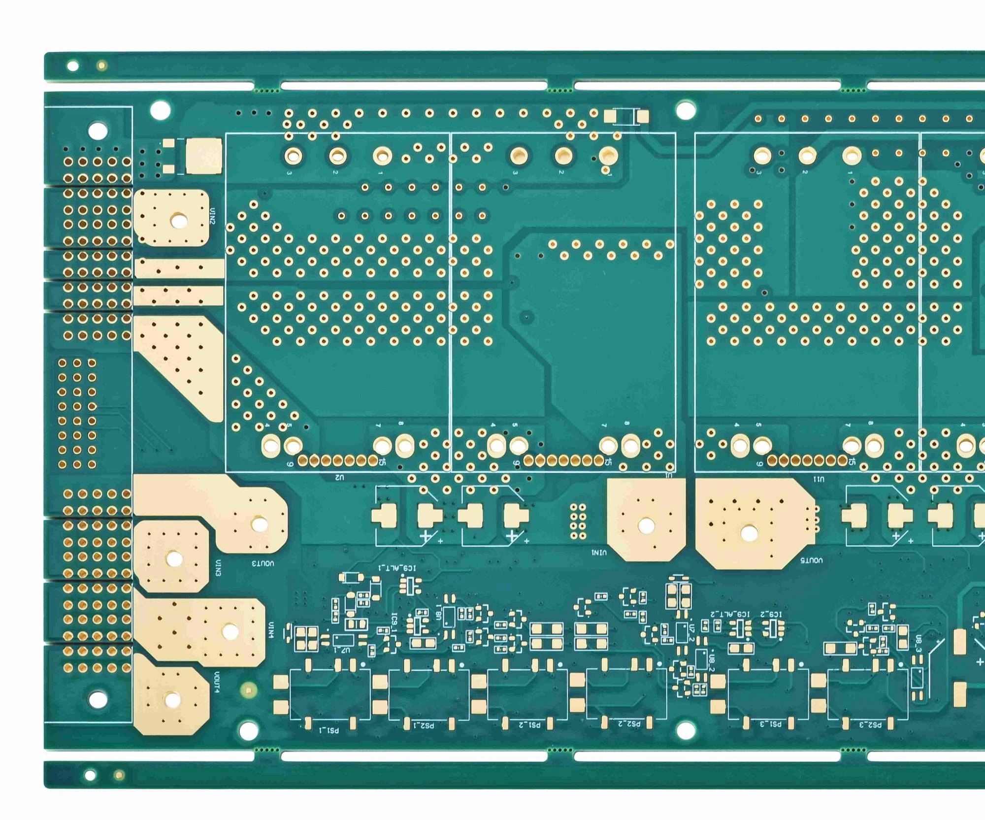
    PCB Z-axis CTE describes how a laminate changes thickness as temperature changes. For a multilayer board with plated through holes, that movement matters because the glass and resin expand different...
  4. PCB Copper Roughness: Skin Depth and Conductor Loss
    PCB Copper Roughness: Skin Depth and Conductor Loss

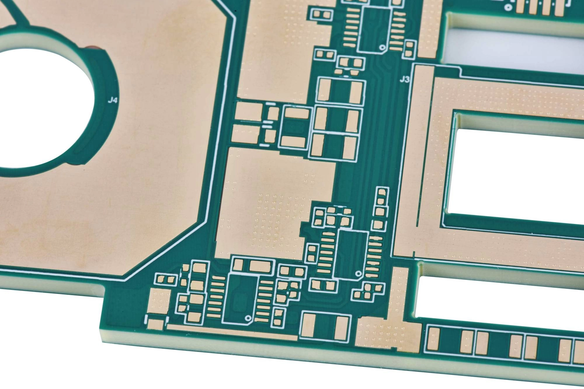
    PCB copper roughness and skin depth describe two different things. Skin depth is a calculated distance inside a conductor at a given frequency. Roughness is measured from a copper surface with a def...

  1. PCB Backdrilling: Residual Stubs and Depth Tolerances
  2. Medical Sensor PCB Design for Low-Noise Inputs
  3. EV Inverter Gate Driver PCB: Local Loops and Isolation
  4. BMS PCB Design Requirements: Sensing and Fabrication
  5. Double Sided Metal Core PCB: Layers and Hole Isolation
  6. Telecom PCB Manufacturing: Release the Critical Channel
  7. RF PCB Supplier Evaluation: Check the Build Evidence
  8. PCB TDR Impedance Test: Read the Lot Report
  9. ENIG Black Pad: Inspection and Lot Traceability
  10. Single-Sided vs. Double-Sided PCB: Routing and Cost
  1. <
  2. 1
  3. 2
  4. >
Send Message
Name*
Email*
Company Name*
Address
Job Title
Phone Number