
A BMS schematic can separate the current-sense signal from the load current, yet the PCB footprint can join them again. A copper pour touching the sense pickup includes part of the power path in the measurement. A later layout revision may introduce that connection without changing the schematic net names.
BMS PCB design requirements therefore need to describe physical paths as well as electrical nets. The bare board must preserve where a measurement begins, which returns it shares, and which conductors remain separated. This review covers fabrication and layout handoff; component qualification, firmware protection limits, and battery-pack validation require their own work.
Contents
A cell-monitor board, a pack-current sensing board, and a controller that communicates through an isolation barrier do not carry the same currents or span the same potentials. Identify the board’s role before specifying heavy copper everywhere. Local cell-to-cell voltage and total pack voltage may govern different areas.
Mark the connector pin sequence and each circuit’s electrical domain. Distinguish cell taps, temperature inputs, balancing paths, power feeds, communication, and current-sense inputs. Include normal operating potentials and the fault conditions used by the system designer. A blanket label such as “high-voltage BMS” hides the location of the stress.
The KnownPCB power-electronics manufacturing page provides the application context for reviewing BMS boards. The manufacturing request should describe the actual circuit roles rather than assume that every board in a battery system needs the same stackup, copper weight, or inspection plan.
For shunt sensing, the measurement starts at defined points on the resistor terminals. Route the low-current sense connections from those points to the input network. A wide load-current connection and a thin sense trace can share a net name, but their branching position determines whether extra copper and solder resistance enter the reading.
Analog Devices’ shunt pad-layout study shows that pad geometry and the sense location affect low-value shunt measurements. Treat the recommended footprint as part of the selected component and accuracy design. Copying a generic four-wire symbol does not establish the correct pickup position for every two-terminal or four-terminal resistor.
Check the final copper after pours and thermal-relief rules have been applied. A pour can reconnect a split pad. An automatic neck-down can move the pickup to a different location. Inspect both charging and discharging current paths, and retain a marked image of the approved shunt region with the fabrication release.
Where parallel shunts are used, current distribution and measurement pickup require a coordinated design. Do not connect sense traces to a convenient outer corner and assume it represents the voltage across every parallel element. Follow the chosen sensing circuit and component guidance, then validate the assembled measurement.
The bare-board photograph below illustrates the coexistence of large conductive features and fine lands. It is not a documented BMS implementation, a Kelvin-routing example, or evidence of a particular measurement accuracy.
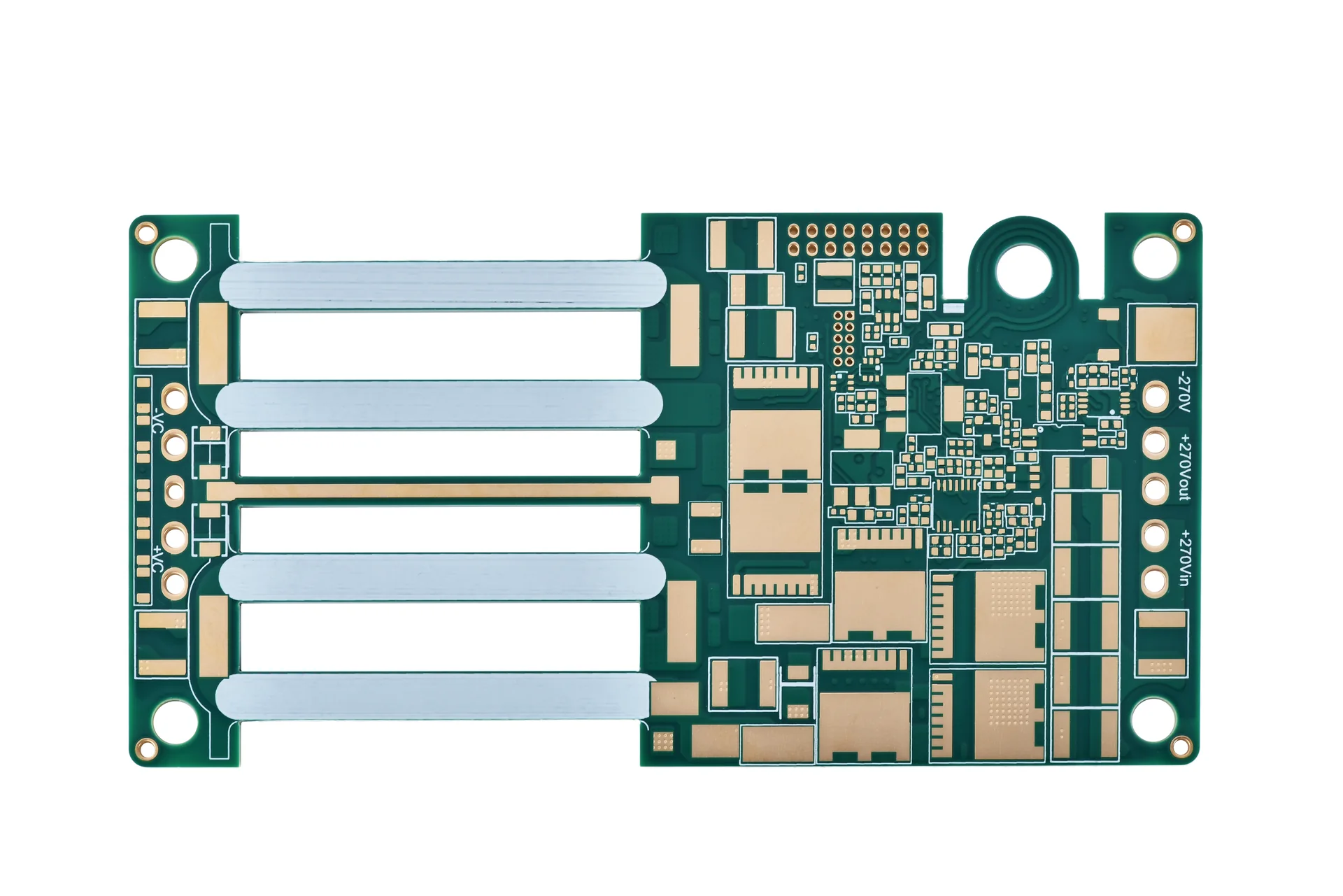
This bare-board example shows mixed large and small features; it is not evidence of a qualified BMS design.
Texas Instruments’ BQ76952 layout guidance calls attention to Kelvin connections and places the differential current-input filter near the monitor. These recommendations are specific to that device. Use the current revision for the selected monitor instead of transferring component values or pin rules from another family.
Keep the two sense routes close together through the relevant region so they encounter similar interference. Avoid a route that sends one input beside a switching node and the other across a quiet plane. Filter placement and the reference connection must follow the monitor circuit, not a universal rule to split every ground plane.
Cell-tap routes also need controlled surroundings. Balance-current traces, connector power feeds, and switched supplies should not share narrow conductive sections with sensitive measurement references. Place the analogue input network so its return path remains local and so component pads and vias can be fabricated consistently.
Review all copper layers, including pours hidden beneath the monitor. An apparently quiet top-layer route can couple to a noisy feature on another layer. A slot or plane gap introduced for isolation can also force a return current around an unintended detour. Resolve those interactions on the complete stackup.
Reserve test access according to the measurement plan. Large exposed probe features on a sensitive node can add a coupling area or leave an accessible energized point. Agree their geometry and location with the validation team before treating test pads as harmless additions.
Passive balancing creates local heat around resistors and their copper connections. Identify which channels can operate together and how the enclosure removes that heat. The board team needs those conditions to evaluate copper distribution and material exposure; the number of cell channels alone does not define the thermal load.
Keep temperature-sensing locations meaningful. A sensor intended to measure a cell should not mainly follow the heat from a nearby balancing resistor unless the system design accounts for that relationship. Mechanical attachment and the thermal path between board and cells are part of this decision.
Mark required isolation zones on every relevant layer and around connectors, mounting hardware, and routed edges. The electrical designer must supply the applicable separation requirements. A board fabricator can review whether the specified geometry is manufacturable; it cannot infer the complete battery-system insulation requirement from Gerbers.
Where slots are required, define the finished width, length, end geometry, and copper clearance. Include nearby components and assembly support. A slot that helps one electrical path may weaken a connector area or remove a return path from another circuit.
Bare-board electrical test checks an agreed netlist. It does not demonstrate state-of-charge accuracy, balancing behaviour, or pack protection. The fixture photograph below represents this limited fabrication inspection stage, rather than functional BMS testing or high-voltage qualification.
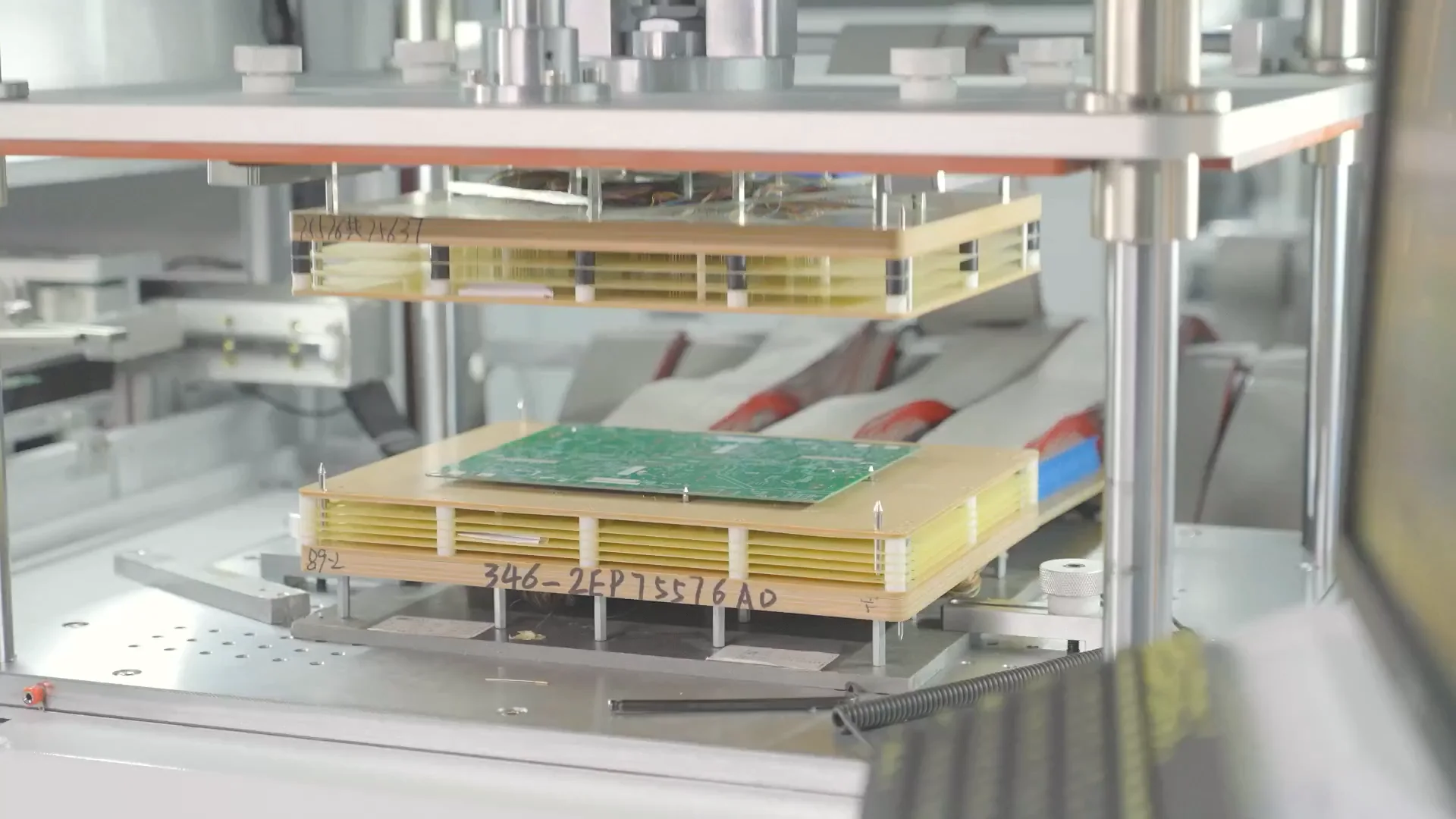
Bare-board electrical testing checks the agreed netlist; this image does not document a dielectric-withstand test.
The existing battery current-sense PCB case article discusses a specific sensing application. For a new BMS, retain the selected device footprint and its own measurement budget. Do not transfer the case’s numerical ratings, claimed resolution, or test conditions into a different product specification.
The release package should identify the stackup, material, finished copper, drill data, netlist, controlled slots, shunt pickup geometry, and approved copper artwork. Include a short map of sensitive areas where a manufacturing query must return to engineering before artwork is changed.
After CAM questions are resolved, compare the approved fabrication data against that map. Confirm that pad splitting, thermal connections, hole tenting, and isolation keepouts remain as intended. Store the reviewed revision with the purchase order so a repeat lot can be built to the same definition.
Use a BMS bare-board manufacturing review to resolve these construction details before release. Include current paths and electrical domains with the files. That allows fabrication questions to be answered without silently changing the measurement topology or claiming that a bare-board inspection validates the complete battery system.
October/09/2026ENIG Black Pad: Inspection and Lot Traceability
October/06/2026PCB Desmear Process: Resin Smear Removal Before Plating
October/22/2026RF PCB Supplier Evaluation: Check the Build Evidence
December/05/2025Automotive Camera Modules (ADAS) HDI PCB Solution
September/28/2026PCB Plating Voids in Through Holes: Causes, Evidence and Prevention