You cannot diagnose ENIG black pad from pad color alone. The term describes localized corrosion of the nickel-phosphorus layer during immersion gold plating. The condition may become visible only at a solder interface or after the gold layer is removed. A sound review brings the cross-section, plating records, sample location, and lot information together.
The recommendations apply to bare-board surface finish and quality records. They do not define an assembly-level acceptance plan or treat a solder joint or finish change as proof of the cause.
Table of contents
ENIG consists of an electroless nickel-phosphorus layer and an immersion-gold layer over a copper pad. The immersion reaction consumes a small amount of nickel as part of the process. Black pad refers to excessive local corrosion of the nickel layer. That corrosion can disrupt the interface and weaken the bond between the solder and nickel-phosphorus layer.
Corrosion does not come down to one bath setting. Gold-bath activity, bath condition, pretreatment, and the uniformity of the nickel-phosphorus deposit can all affect the interface. Under the specific cyanide-electrolyte conditions in a published corrosion experiment, local differences in phosphorus content across the Ni-P layer created a potential difference and promoted localized corrosion. The result shows that composition distribution can contribute to some corrosion reactions. It does not establish phosphorus variation as the sole cause of every black-pad lot. See the corrosion study for its test conditions.
IPC-4552B covers ENIG deposit thickness, measurement, process control, and nickel-corrosion evaluation in separate sections. Check which revision and purchase requirements apply to the project. Do not treat a thickness value copied from a web article as a universal acceptance limit. The public IPC-4552B table of contents shows the scope of the specification.
The name black pad suggests a dark pad, but the gold or silver-yellow color on a bare board does not confirm whether the nickel layer has corroded underneath. The gold covers the nickel-phosphorus layer. A photograph usually records surface color and reflection, not the condition of the interface. IPC lists corrosion evaluation, cross-section inspection, and deposit measurement as separate subjects. Color cannot replace an interface examination.
Poor wetting, brittle separation, or an intermittent BGA open after soldering can trigger a failure analysis, but none proves that black pad is the cause. Solder paste, storage, thermal stress, board flexure, and other surface conditions can also affect a joint. To attribute the failure to an ENIG interface, inspect the nickel and gold structure at the affected location.
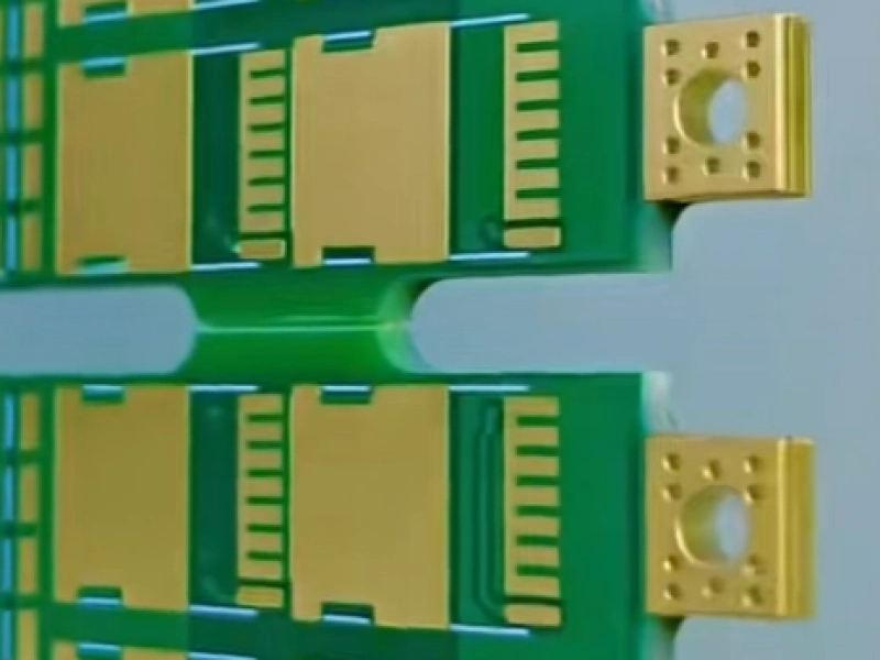
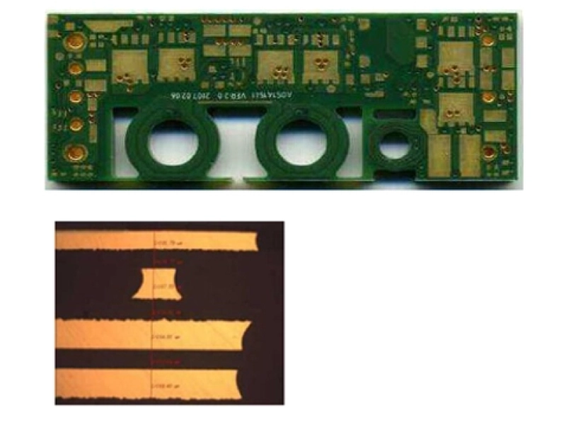
The images below show finished ENIG pads and board surfaces. They are not black-pad photographs and cannot be used to diagnose the defect.
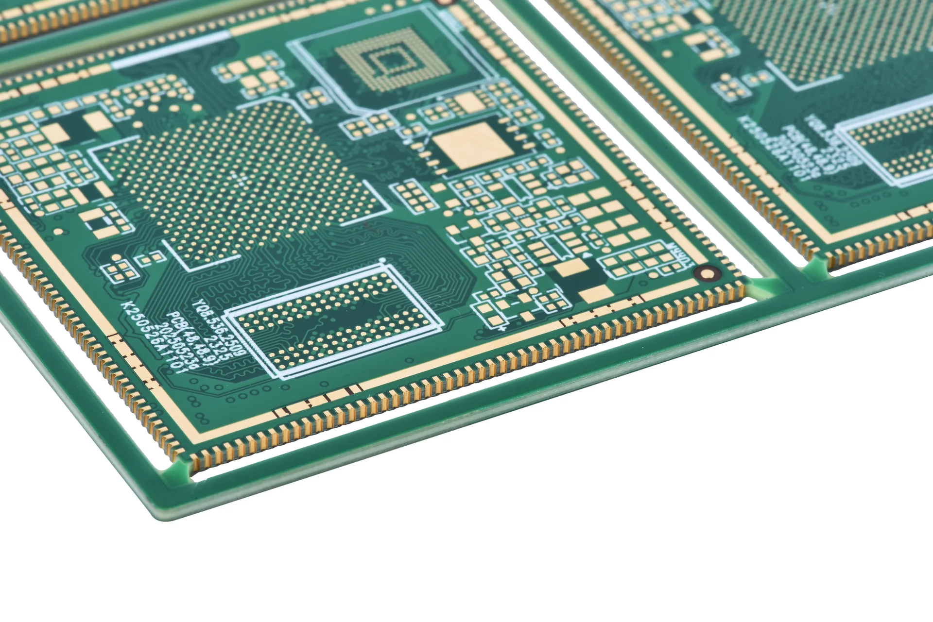
ENIG castellated-hole PCB. This product photo does not show nickel corrosion or a black-pad defect.
Start by identifying the sample. Record the board number, panel position, pad coordinates, finish requirement, delivery lot, and the process stage where the issue appeared. If the concern appeared after soldering, retain the failed assembly, an unassembled board, and a control sample from the same lot. Similar interface morphology at several locations in one lot can change the scope of the investigation.
A cross-section can show continuity at the copper, nickel-phosphorus, and gold interfaces, and can link corrosion morphology to the solder separation surface. Record the section location and direction, preparation method, and interpretation basis. A dark residue seen after scraping a pad is not enough to call it black pad. Prepare the section using the agreed method and assess it against the IPC revision and acceptance criteria that apply to the project.
XRF can measure gold and nickel thickness, but it does not by itself reveal interface corrosion morphology. If a customer specification calls for nickel-phosphorus composition data or a more detailed interface examination, first confirm that the sample, instrument method, and report fields are suitable. Each method answers a different question. A passing thickness result does not equal a passing corrosion evaluation.
Texas Instruments notes in its application report on ENIG package solder joints that external inspection cannot identify affected material and discusses destructive analysis such as microsectioning. That report covers semiconductor packages and post-assembly joints. It is not a universal bare-board acceptance plan. Bare-board sampling should follow the drawing, customer specification, and inspection plan agreed by both parties. Read TI's application report on ENIG package solder joints with that scope in mind.
A product photo can help locate an issue, but it cannot show magnified interface layers, measurement conditions, or sampling coverage. If a report includes only a close-up of a pad, add the sample ID, location map, and inspection method before deciding whether to section or retest it.
IPC-4552B is a performance specification for ENIG finishes on printed boards. Its scope includes deposit thickness, measurement methods, process control, and nickel-corrosion evaluation. It does not provide a color chart that can identify every black-pad defect, and it does not replace other finished-board purchase requirements.
Before a project starts, state the specification revision, board class, applicable clauses, sample locations, and required report format in the purchase documents. If the customer has additional acceptance terms, identify which document takes precedence. Naming a standard on a drawing without its revision or test method can leave the two parties applying different criteria.
The public table of contents places corrosion evaluation, deposit thickness, XRF measurement, and process control in separate sections. Use the full standard text adopted for the project to confirm limits and test details. Confirm corrosion criteria and test steps against that adopted text, together with the sample preparation method and release requirements.
ENEPIG adds a palladium layer and changes the interface chemistry during gold deposition. Whether to use it depends on the product requirements and the full specification. It is not an absolute guarantee against every interface defect, and finish selection does not replace evidence gathering and lot traceability. See KnownPCB's existing ENIG and ENEPIG comparison for differences in intended use.
KnownPCB's ENIG PCB page describes its surface-finish service. For the board material, finish, and inspection documents, the quality management page can help frame which records to discuss. A page description does not mean that every order includes a specific corrosion test. Put the acceptance items in the purchase documents.
When an abnormal sample arrives, first identify its board number, lot, and finish route. Compare these details with that lot's outgoing inspection, thickness data, instrument calibration status, and available process records. If you request bath-maintenance, chemistry, or process-change records from the supplier, record each document date, sample ID, and data range. Do not present an assumption as a confirmed root cause when the records are missing.
For a review, select samples from different panel positions in the same lot and, when useful, a neighboring lot. Set the sampling plan before comparing results so the review does not focus only on the most visible pad. If the interface morphology is consistent across samples, the investigation may need to cover the corresponding lot or process interval. If results differ, check the sampling location, section direction, and measurement repeatability.
A reviewable record links the sample source, finish specification, measured data, cross-section images, equipment and method, acceptance basis, and lot reference. A note that says only "black pad found," without coordinates, original images, or inspection steps, is difficult to reproduce. Use the records to agree with the supplier on whether to contain material, repeat a test, or expand sampling.
Keep original images and records rather than saving only cropped close-ups. A traceability table can connect the customer part number, board number, panel number, production lot, inspection date, and section ID. If different areas of one panel show different features, mark the locations before comparing them. That helps distinguish a local finding, sampling variation, and a process-lot pattern.
Separate observations from conclusions. "The section shows continuous corrosion morphology at the pad edge" describes an observation. "The entire lot is nonconforming" requires support from the sampling plan and applicable criteria. Decisions to quarantine, rework, or scrap material belong to the parties' contract and quality procedures, not to a single photograph.
This multi-up ENIG board photo shows panel layout and pad distribution, not the nickel interface or a finish measurement.
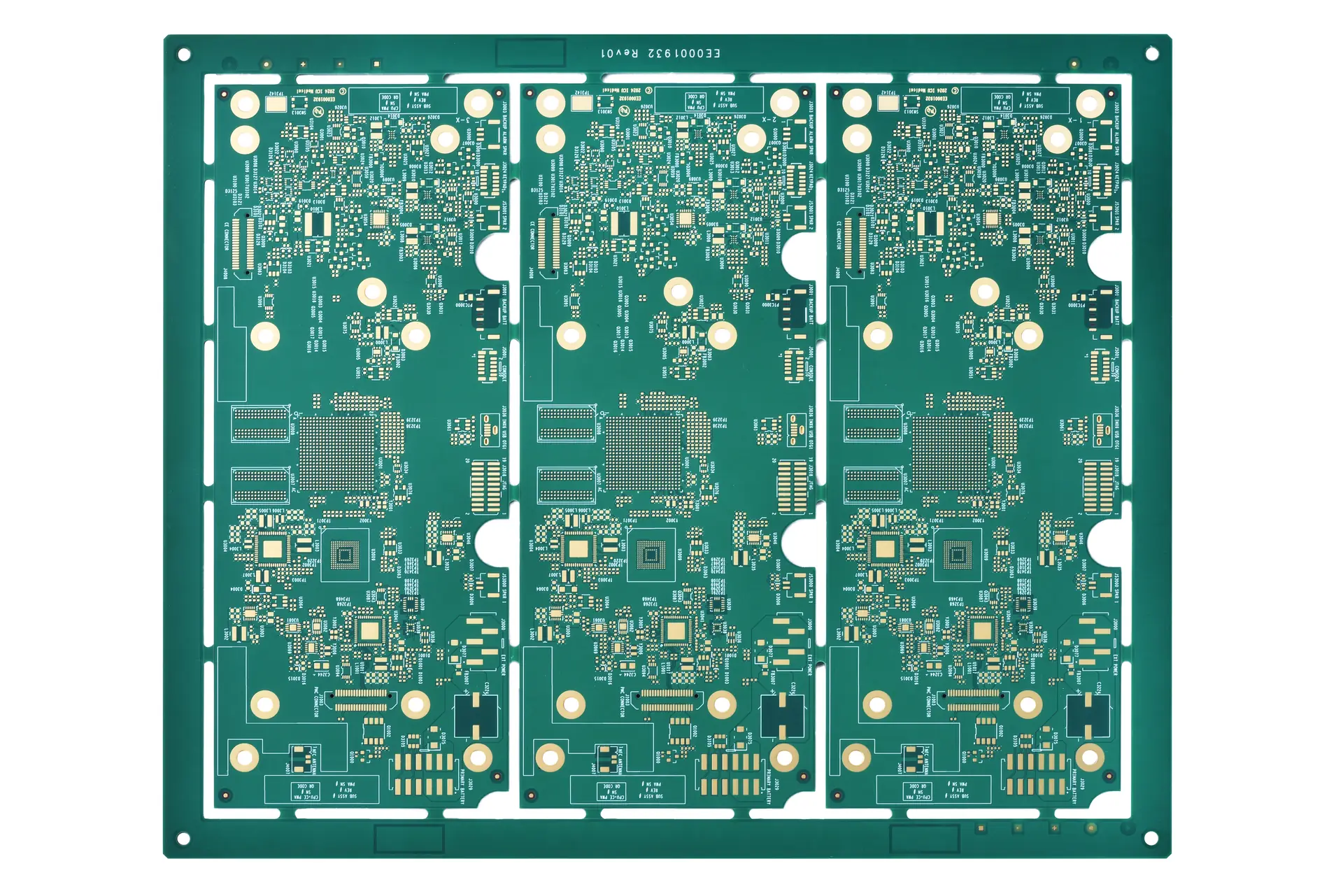
Multi-up ENIG PCB. This product photo does not show black pad or another surface-finish defect.
At the design stage, put the ENIG specification revision, intended use, sampling requirements, and required reports in the drawing and purchase documents. For an existing issue, send the Gerber files, finish notes, lot number, and marked defect location to the KnownPCB engineering team for a bare-board DFM and inspection-record review.
No. The gold covers the nickel-phosphorus layer, so a surface photograph cannot show the underlying interface. A color change can be recorded as a reason to inspect further, but it cannot establish the defect by itself. Check cross-sections, deposit measurements, and lot records against the project specification.
No. One location is not enough to extend the conclusion to a whole lot, but a single visible location does not rule out a lot-level process issue. Confirm the sample lot and position, then inspect different locations in the same lot under the agreed sampling plan. Expand containment or testing only when the evidence supports it.
The palladium layer in ENEPIG changes the interface conditions during gold deposition and can reduce a specific nickel-corrosion path. It does not mean that every failure mode is eliminated. Select the finish for the product use, assembly requirements, and agreed specification, and retain the related process and inspection records.
Texas Instruments, Use and Handling of Semiconductor Packages With ENIG Pad Finishes, SPRAA55, 2004.