
A drawing that says only "gold finish" leaves the fabricator with a choice the buyer may not have intended. ENIG has nickel and immersion gold over the copper pad. ENEPIG adds palladium between them. The added layer changes the process record and the checks a buyer should request.
Specify what the pad must do. A solderable pad, a wire-bond pad and a contact pad can require different evidence even when the finished surfaces look alike. This is a bare-board finish decision; the drawing should name the finish and the tests required for its intended use.
Table of Contents
ENIG means electroless nickel followed by immersion gold. Nickel is deposited onto the exposed copper, and the thin gold layer protects the nickel surface before the board is used. ENEPIG means electroless nickel, electroless palladium and immersion gold in that order. The palladium sits between nickel and gold. The public scope of IPC-4552B for ENIG and IPC-4556 for ENEPIG describe these layer structures and the performance functions that the specifications address.
A gold-colored board photograph cannot identify the complete layer stack. Both finishes can look similar from above. A buyer needs the approved surface-finish callout and inspection record, not only an image or the supplier's shorthand term "immersion gold." If a drawing says ENIG, adding palladium without agreement changes the specified finish. If it says ENEPIG, an ENIG certificate does not prove the palladium layer exists.
| Finish | Metal stack over copper | Specification to confirm |
|---|---|---|
| ENIG | Electroless nickel, immersion gold | The order's stated IPC-4552 revision and exceptions |
| ENEPIG | Electroless nickel, electroless palladium, immersion gold | The order's stated IPC-4556 revision and exceptions |
KnownPCB's ENIG PCB page describes its ENIG product offering. It does not, by itself, verify that a particular order can be supplied with ENEPIG. Confirm that capability with engineering before putting ENEPIG on a delivery promise.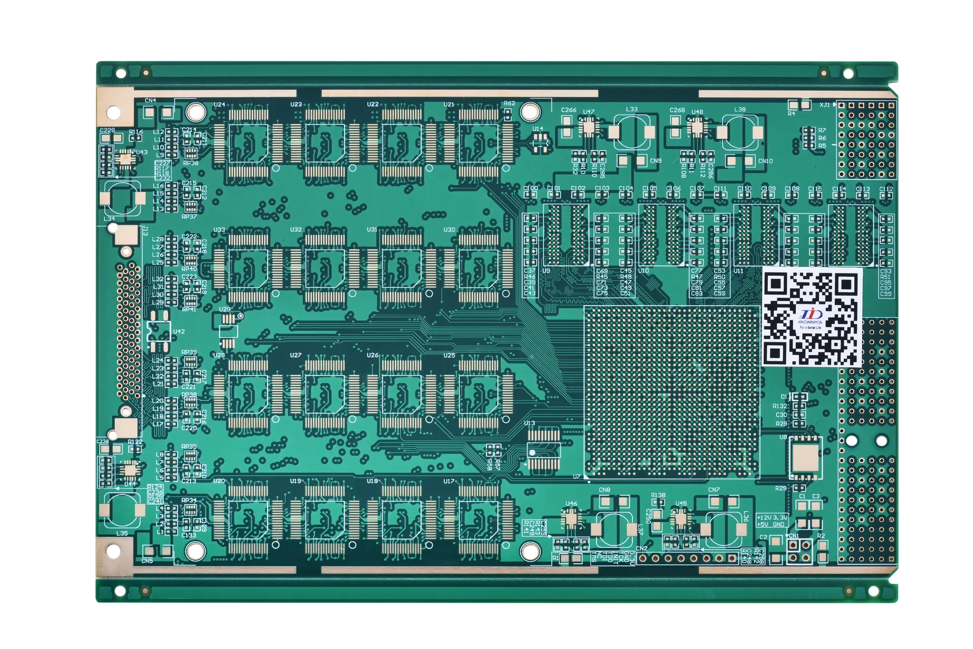
This is an ENIG board. The photo cannot show whether a palladium layer is present on another board.
ENEPIG's palladium layer separates nickel from the immersion-gold step. It limits direct attack on the nickel during gold deposition and provides a surface used in specified bonding processes. A board that needs both soldering and wire bonding is one reason to assess ENEPIG.
The palladium barrier still has to be deposited correctly. Nickel, palladium and gold thicknesses, cleanliness and the interfaces between them remain part of the process check. ENIG can also support certain bonding methods, so the wire material and bonding process must be named before ruling it out. A BGA or QFN package name alone does not settle the finish choice.
For ordinary solderable pads, a qualified ENIG process can be an appropriate choice. ENEPIG becomes more relevant when the same board must also meet a defined gold-wire, aluminum-wire or copper-wire bonding requirement, or a contact requirement covered by the selected specification. The exact bonding process belongs in the drawing and purchase order; "wire bondable" alone is too vague for a fabrication quotation.
Fine-pitch pads need an even finished surface, but pitch alone does not choose between ENIG and ENEPIG. Repeated-mating connector fingers raise another question: thin immersion gold is not automatically a substitute for specified hard gold. Mark pads with different functions on the drawing, then ask the fabricator to review the masking and finish sequence. KnownPCB's surface-finish comparison covers ENIG and hard gold separately.
| Requirement on the drawing | Finish review | Evidence to request |
|---|---|---|
| Solderable bare-board pads | Compare qualified ENIG and ENEPIG routes against the actual order. | Finish callout, thickness results and solderability requirements. |
| Soldering plus specified wire bonding | Review ENEPIG and the exact bonding process; do not assume every ENIG process fails. | Wire material, bond method, qualification sample and test criteria. |
| Repeated-mating connector fingers | Check the contact specification separately; thin immersion gold is not automatically hard gold. | Mating-cycle requirement and approved contact finish. |
A dense HDI layout may have many small finished pads, but it does not establish a wire-bonding requirement. The intended joining process still determines the finish specification.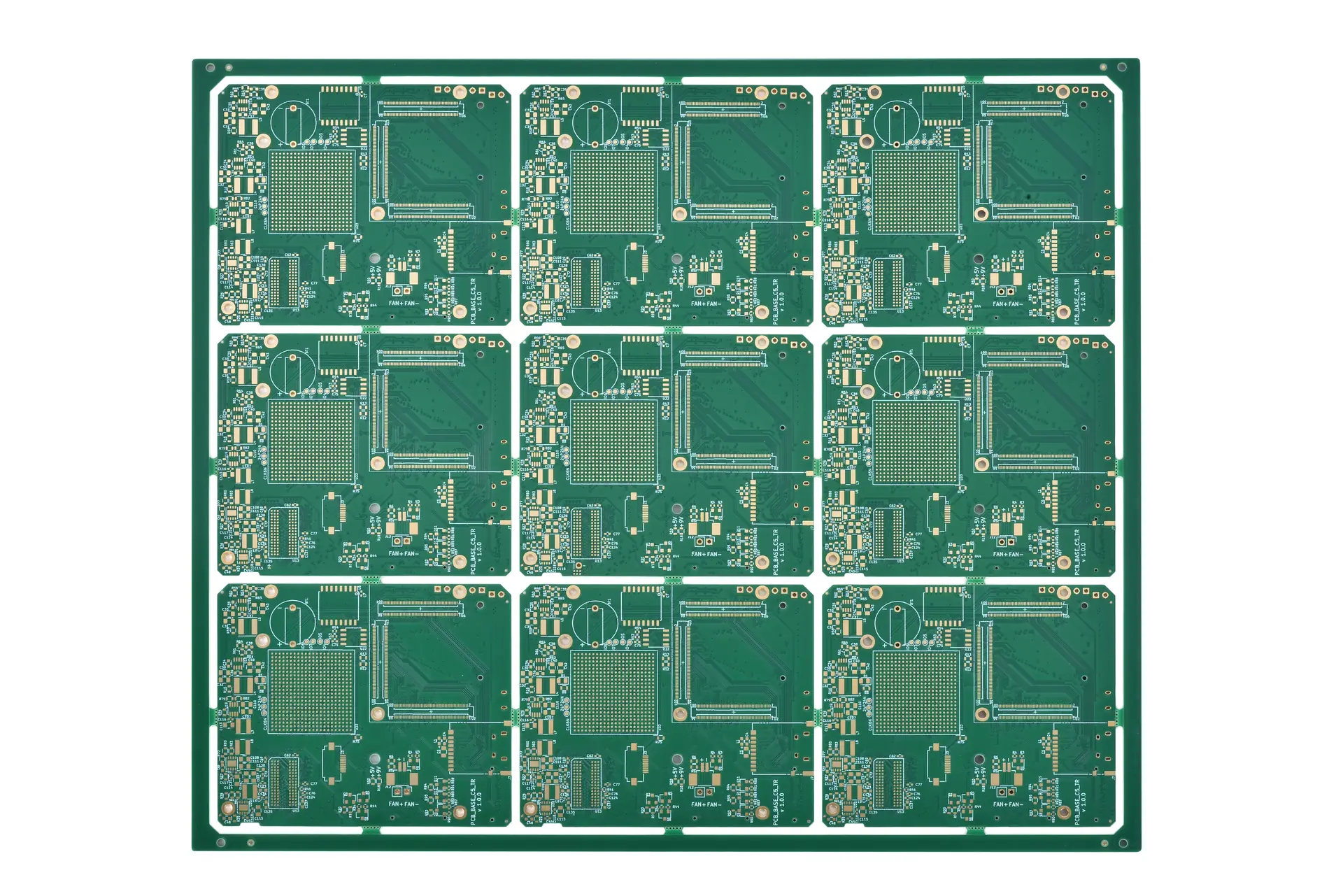
An ENIG-finished HDI panel can have fine-pitch pads. The pad function, not pitch alone, determines whether ENEPIG should be considered.
Some ENIG failures associated with excessive nickel corrosion are often described as "black pad." The term is a warning to investigate the nickel and gold interface, not a visual diagnosis from a dark photograph. IPC-4552B includes nickel-corrosion evaluation and process-control provisions. A supplier claiming conformance should be able to identify the specified revision, test plan and results for the relevant lot.
The palladium layer in ENEPIG changes the path by which the immersion-gold step interacts with nickel. It can reduce a known ENIG risk, but it does not establish zero risk of every soldering or bonding defect. IPC-4556 includes requirements for the three-layer deposit and performance tests. When a customer's application is sensitive to bonding strength, the purchase documentation should call out the required coupon, test and acceptance criteria instead of relying on the finish acronym alone.
A photograph records pad color, not nickel corrosion level or palladium thickness. A normal-looking pad may still need a section or thickness result under the agreed inspection plan. If a pad looks unusual, record the location and examine it; color alone does not name the defect. KnownPCB's quality-management process describes the broader inspection and traceability controls.
ENEPIG adds a palladium bath and another layer to control. A quote therefore needs the finished area, target deposit thicknesses, sample plan, panel design and order quantity. A fixed percentage premium from a blog is not a reliable substitute for those details. If the design otherwise needs a separate finish for bonding pads, compare the complete board routes rather than the price of one bath.
Ask where each finish step will be performed and which thickness or qualification records will ship with the boards. A subcontracted step can be acceptable if the approved process and traceability remain intact. KnownPCB's site confirms an ENIG offering, but it does not confirm an ENEPIG line for this order. Engineering should verify that capability before quoting ENEPIG.
Provide Gerber or ODB++ files, the stackup and a fabrication drawing that calls out ENIG or ENEPIG by name. Mark any selective-finish areas. State the IPC specification and revision required by the purchase order, plus any agreed exceptions. If wire bonding is involved, state the wire material, bonding method, pad locations and qualification tests. For contact pads, add the electrical or mating requirements rather than writing only "gold fingers."
The engineer can then check pad geometry, solder mask openings, finish coverage, measurement coupons and the supplier's qualified route. For a bare-board quotation, a BOM or component-placement file is not a substitute for the finish callout and drawing notes. Ask KnownPCB to review the finish specification
No. Both finishes can serve solderable PCB pads when their processes meet the specified requirements. ENEPIG adds a palladium layer and may be useful for a defined bonding or contact function. The order's pad function and qualified process determine the choice.
No. Palladium changes the nickel-to-gold interface and can reduce one known corrosion mechanism. The three deposits still need process control and the required inspection evidence.
No. The finishes can look similar from above. Confirm the metal stack through the fabrication callout, production record and appropriate layer-thickness measurements.
IPC-4552B, ENIG Plating for Printed Boards, public scope and contents.
IPC-4556, ENEPIG Plating for Printed Circuit Boards, public scope and contents.
March/10/2026How 0.2–1.2 mil Solder Mask Thickness Affects 100 Ω Differential Impedance and Insertion Loss
March/24/2026HDI Microvia Cracking | Failure Analysis Steps

September/28/2026PCB Desmear Process: Resin Smear Removal Before Hole Plating
April/09/2026Heavy Copper PCB Projects
April/24/2026Aluminum vs Copper vs Stainless Steel MCPCBs: Thermal Performance, Cost and Applications
