
PCB etch compensation is an adjustment to production artwork that helps an etched conductor reach its specified finished width. A designer releases the width the board needs. The fabricator prepares the pattern that will produce it on the selected copper and process. The useful question in a drawing review is which width each person is looking at.
On this page · Three widths · Side etch · Section measurement · Drawing notes
Released width. The nominal conductor geometry in the design data, read with the fabrication drawing and applicable tolerance.
Production artwork width. The feature prepared in CAM for the imaging and etching route. It may include an allowance for material removed during etch.
Finished width. The physical conductor dimension at the agreed location and measurement plane.
Start with the released files and drawing as one package. If an impedance table specifies a finished width that differs from the supplied copper artwork, ask engineering to resolve the difference before tooling. An example controlled cross-section drawing from Altium shows how a drawing can authorize manufacturing allowances in working artwork while holding the finished geometry to the design requirement. Use your own tolerance and approval language for the actual job.
 Rows of PCB etching equipment with enclosed conveyor sections](/upload/image/20261113/des-etching-line-01.webp "[des-etching-line-01.webp](/users/mac/desktop/knownpcb/batch-2026-11-11-next8/media/k19/des-etching-line-01.webp) rows of pcb etching equipment with enclosed conveyor sections")
Developing and etching equipment in the outer-layer patterning area.
In a subtractive process, a resist protects the copper pattern while exposed copper between features is removed. Etching can also remove copper laterally from the exposed sidewalls. The protected trace can therefore have a narrower top than base. The actual profile depends on the process and the layer construction, so a width observed at the top and a width measured at the laminate interface describe different parts of the same trace.
CAM can widen a protected feature to account for side removal. That change also uses space in the production pattern. Copper thickness and the open spaces next to a conductor matter because the process must clear copper between features while preserving the lines beside them. Altium’s trace-width design discussion explains why a thicker copper layer can change what narrow features can be produced repeatedly.
Illustrative geometry at a fixed pitch
Take two 140 µm artwork traces on a 270 µm center-to-center pitch. Their nominal gap is 130 µm. If a CAM example adds 7 µm on each side of each trace, the compensated width is 154 µm and the artwork gap becomes 116 µm. These example dimensions show how a width change consumes space. The finished gap and the allowable compensation depend on the approved route and acceptance dimensions.
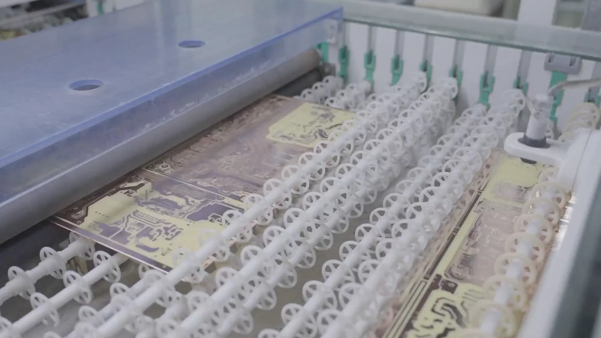
A patterned panel moves through the outer-layer etching line.
A plan view gives the route and spacing. A cross-section can show the conductor height and the widths at different levels. Altium’s routing impedance cross-section notation defines etch factor as copper thickness divided by half the difference between bottom and top widths for a symmetric trapezoid. For an illustrative 35 µm-high conductor with a 150 µm base and a 130 µm top, the inferred lateral difference on each side is 10 µm and the ratio is 3.5. Record the measurement convention and units when comparing results from two reports.
For controlled impedance, send the trace layer, reference layer, target and tolerance, and the mask condition near that trace. Width and spacing are only part of the cross-section. Copper height and the finished dielectric distance to the reference plane also affect the result. If an engineer proposes changing width to meet the impedance target, review the new gap at nearby pours, the pair spacing, and transitions at pads before approving it. The controlled-impedance fabrication requirements help define the handoff.
Ask which features the inspection will check. An optical pattern comparison can flag missing or excess copper. A section through an agreed representative feature can show its profile. If width at a specific height is critical, describe the section location and width reference on the drawing instead of asking for a generic inspection photo.
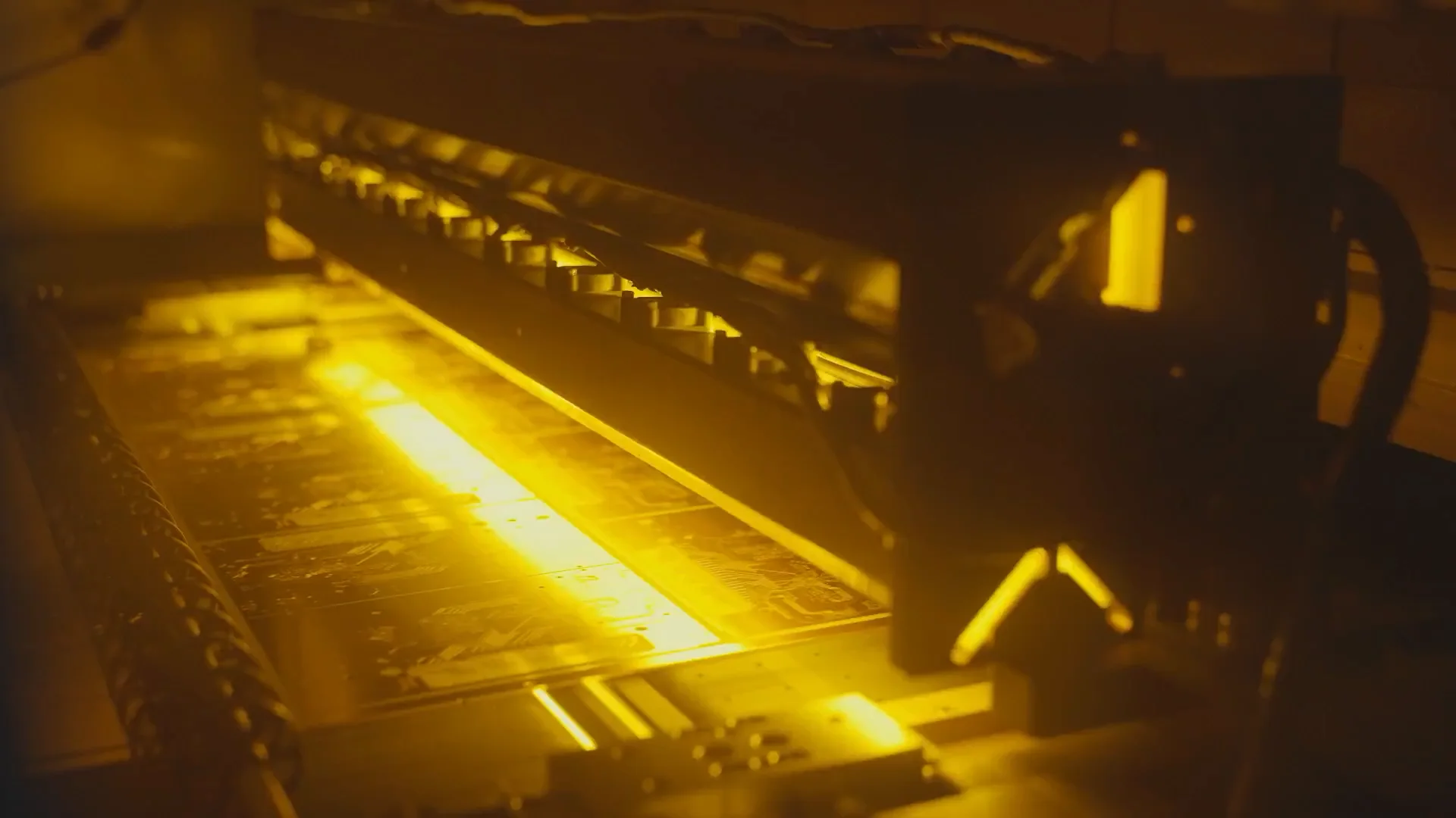
Optical inspection of the copper pattern.
When a report lists one width for a coupon and another for a functional trace, check which locations were sampled. A coupon with a different copper thickness, neighboring pattern or reference plane can answer a different question. Agree on what the coupon represents and what needs to be measured directly on the board.
Write the width requirement where the CAM engineer can reconcile it with the layer artwork. A line that carries a large current and a line in an impedance-controlled pair can need different acceptance criteria even when their nominal widths are the same. Identify the relevant layer and feature by a drawing detail, net or location. Keep the specified finished copper thickness in the same stackup revision.
What to send for a compensation review
Released copper data and drawing revision, the affected layer and feature, finished width and spacing requirements, the inspection plane and any impedance constraint. State which changes need approval and who can authorize them.
For a dense board, show the narrowest location next to the trace and the surrounding copper, not just an isolated width callout. During a multilayer PCB fabrication review, the fabricator can use the complete design context to propose artwork changes and identify any geometry the design owner needs to approve.
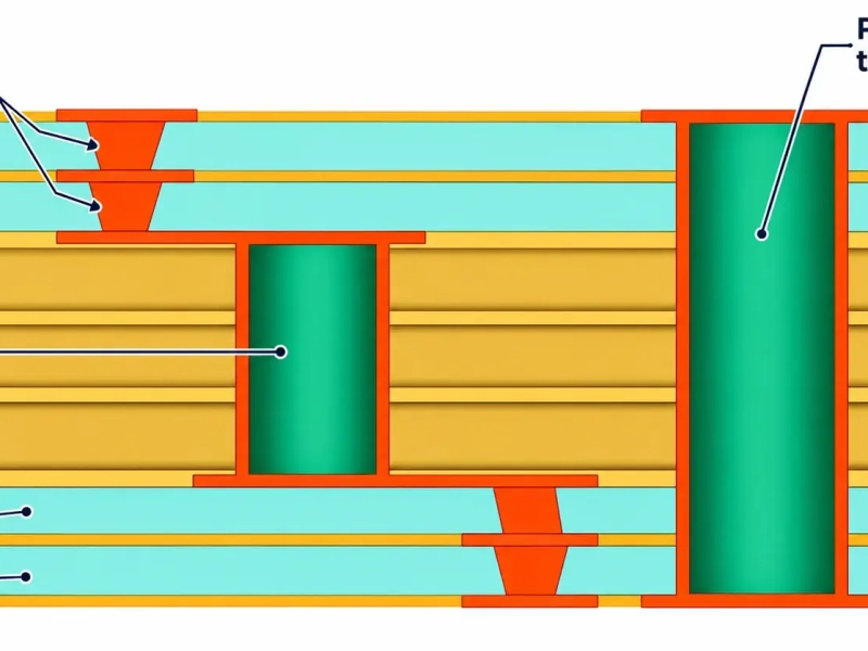
November/12/2026PCB Assembly DFM: Practical Rules to Reduce Defects
October/30/2026112G PAM4 PCB Design: Baud Rate and Channel Budgets

December/05/2025Automotive Camera Modules (ADAS) HDI PCB Solution
November/13/2026Flying Probe vs Fixture Testing for Bare PCBs
December/06/2025What Are The HDI Board Risks for Radar Modules