
PCB Assembly DFM: Practical Rules to Reduce Defects
Most PCB assembly defects don't start from the production line. Industry data indicates that over 60% of PCBA issues come from early design decisions. When these issues appear only in pilot or mass production, the average cost to rectify them is more than 10 times higher than it would have been during layout.
For instance, in an industrial control board project that using a 0.4 mm pitch QFP, the pads were copied straight from the datasheet and the stencil was left unchanged. After reflow, Automated Optical Inspection (AOI) flagged widespread insufficient solder. The root cause was design—pads were too short for proper wetting and the stencil aperture ratio was too high. We had to respin the board and this resulted in a 2-month delivery delay.
Effective PCB assembly DFM (Design for Manufacturability) prevents such issues before they happen. It is not a final check after routing. It is a set of practical rules you apply from component selection through thermal design.
1. Component Selection for High Yield
Choosing the right package size directly impacts your SMT assembly yield and assembly costs.
- Package Preference: For resistors and capacitors, the prefered order is 0805 > 0603 > 0402 > 0201.
- Avoid ultra-fine pitches when possible: Stay away from QFPs and BGAs with pitches under 0.3mm unless it's necessary for your design. Fine pitch does not mean better engineering. A 0.4mm-pitch QFP may lead to a drop in factory yield of 10%.
- Thermal management: Components with bottom thermal pads—like QFN-EP and PowerPAD, require thermal vias and segmented stencil apertures. Without them, you risk bottom cold joints and excessive solder voiding.
- Verify manufacturer tolerances: Identical part numbers from different suppliers often vary in pin length and coplanarity. Try to build footprints using recommendations from mainstream pcb assembly manufacturers. If a heat-sensitive component conflicts with standard reflow profiles, consider a multi-stage soldering or choose an alternative package.
2. Reliable Pad and Solder Mask Design
Reliable PCB footprint design should base on the IPC-7351B standard, and adjust for the real manufacturing process. The IPC-7351B defines clear naming conventions and dimensional targets. For example, RESISTOR_0603_1608METRIC identifies a 0603 imperial-size resistor with a nominal body size of approximately 1.6 mm × 0.8 mm.
Follow these core rules to prevent solder bridging and open joints:
- Size your pads for proper fillets: Make pad lengths 0.3mm to 0.8mm longer than the component lead to allow clean solder wicking. Make pad widths 0.1mm to 0.2mm wider than the lead to prevent shorts.
- Control solder mask expansion: Keep solder mask openings roughly 0.1mm smaller than the copper pad to stop mask encroachment from ruining solder wetting.
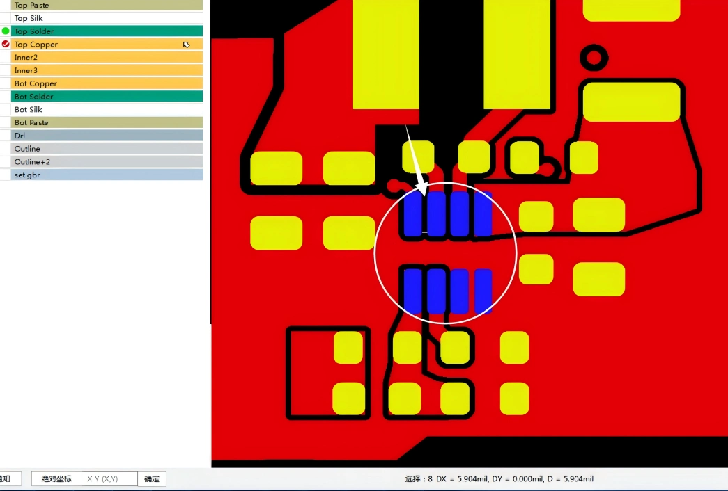
- Enforce solder mask dams: Maintain at least a 0.1mm green solder mask bridge between adjacent, independent pads.
- Use SMD pads for fine-pitch ICs: For dense QFNs and BGAs, use Solder Mask Defined (SMD) pads instead of Non-Solder Mask Defined (NSMD) pads to lock down the solderable area. Never use gang-relief (single large openings) across an entire row of pins.
3. Layout and Spacing
Smart PCB layout guidelines streamline pick-and-place programming and prevent mechanical collisions.
- Group similar components: Cluster identical components together to minimiza feeder swaps on the pick-and-place machine.
- Align component polarity: Ensure all SMD components are in the same direction to speed up visual and automated inspection.
- Plan for mixed technology: Reserve clear wave-soldering keep-out zones on double-sided mixed-assembly boards. And maintain at least 3mm of operational space around large components.
- Placement spacing: Maintain at least 0.2mm spacing for standard SMD components and 0.18mm for precision micro-components. Gaps under 0.15mm block stencil squeegees, cause uneven paste printing, and trigger nozzle collisions.
- Design accessible test points: Place exposed test pads with a minimum diameter of 0.9mm (most ICT probes prefer 1.0mm, though some factories accept down to 0.3mm depending on fixture capabilities). Keep test points at least 0.5mm away from component edges and completely free of silkscreen. Group them in open, low-heat areas away from hot MOSFETs or main processors, and never route traces over them.
Case Study: In a recent telecom module project, engineers placed several BGAs closely together. This caused the assembly to heat up too slowly during reflow, resulting in cold solder joints. After switching to a more distributed layout and incorporating thermal balancing design, the soldering defect rate dropped by 90%.
4. SMT Stencil Design Rules
SMT stencil design,especially foil thickness and aperture ratios usually directly determine the volume of solder paste deposited. Use these baseline targets:
- Stencil thickness: Use 0.10mm to 0.15mm foils, use thinner stencils for fine-pitch ICs.
- Aperture reduction: Size most apertures to 80%–90% of the copper pad area. For large thermal pads, this can be reduced to roughly 70% to minimize outgassing and solder voids.
- Advanced aperture shapes: Use window-pane (crosshatch) or segmented apertures for BGA and CSP thermal pads. For ultra-fine-pitch QFNs, consider nano-coated stencils to improve solder paste release.
For package-specific examples, see Texas Instruments’ QFN and SON PCB attachment guidance.
5. Thermal Management for Reflow Soldering
Uneven heat distribution causes two classic reflow soldering defects: cold joints (where heavy copper planes steal heat from nearby pins) and tombstoning (where uneven heating pulls small passives upright).
- Add thermal relief spokes: Never connect large component pins directly to solid copper pours. Use star-shaped thermal reliefs with 0.2mm to 0.3mm spoke widths, and slightly reduce stencil apertures on those pads to balance heat absorption.
- Balance pad symmetry: Ensure both pads of small two-terminal chips connect to identical copper traces to stop tombstoning.
- Segment large ground pads: Break up massive ground pads using solder mask grids, cross-shaped paste openings, and perimeter thermal vias. This evens out board temperatures across small and large parts, letting your board run on a standard reflow oven profile without custom line tweaks.
For more on the mechanism, see Indium Corporation’s explanation of tombstoning.
Watch tombstoning form during reflow on YouTube to see how a small chip component lifts onto one end.
6. Material and Stackup Selection
Match your PCB stackup and laminate material directly to your operating environment.
- High-frequency RF boards: Use specialized low-loss RF laminates. Standard FR-4 suffers from unstable dielectric constants, which can lead to impedance mismatches, signal loss, and dropped packets.
- High-current power boards: Specify heavy copper weights to handle current loads safely.
- Outdoor and industrial boards: Choose high-Tg laminates. Running high voltage or heavy copper on thin, low-Tg FR-4 would cause delamination and blistering over time, creating serious safety hazards.
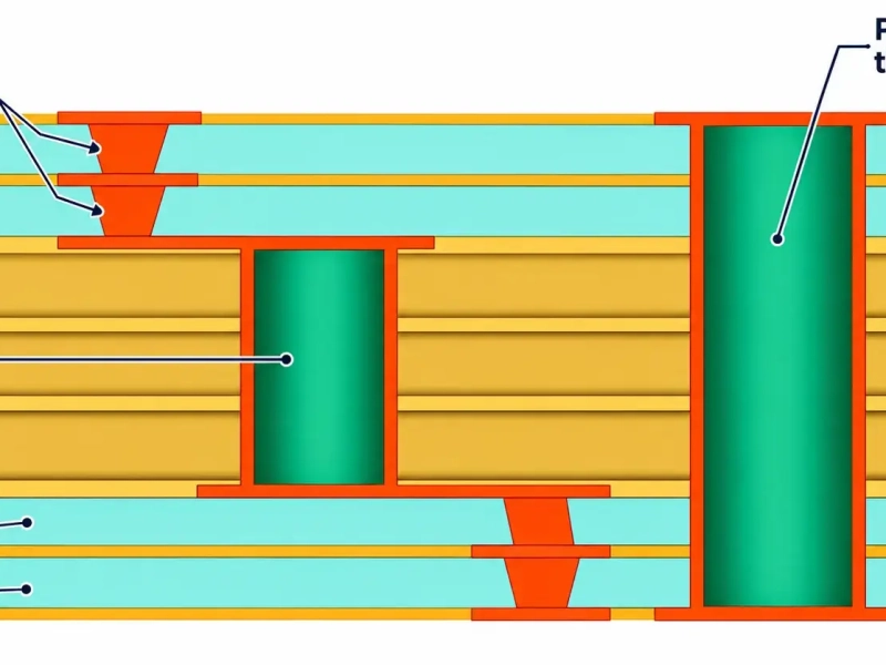
For via structures, materials, and layer planning, see our guide to HDI PCB stackup manufacturability.
How to Evaluate Your Contract Manufacturer's DFM Capabilities
Before sending Gerbers to a PCBA manufacturer, ask these questions to evaluate their defect-prevention process:
- Do you run a formal engineering DFM review on every new order and send back an actionable issue report?
- How do you inspect hidden solder joints on BGAs and QFNs, and do you have in-house X-ray inspection?
- Can you share First Pass Yield (FPY) or Defects Per Million Opportunities (DPMO) metrics for boards of similar complexity?
- How do you manage Moisture Sensitivity Level (MSL) components, stencil storage, and pick-and-place program revisions?
A factory that treats DFM as true engineering—not a mere formality—will be able to catch these costly issues long before cutting a stencil.

Review our quality control and engineering review process when discussing inspection coverage for your project.
Quick Reference – Common Defects and Fixes
| Defects | Root Cause | DFM Action |
|---|---|---|
| Solder balls | Oversized apertures + insufficient preheat | Reduce aperture to ~85% and extend the reflow preheat zone. |
| Component shift | Unbalanced pad forces | Match pad dimensions and copper trace widths symmetrically on both ends. |
| High BGA voids | Poor thermal-pad via and aperture design | Use micro-via array + segmented openings |
| ICT test failures | Test points too small or blocked | Add dedicated 1.0mm exposed copper test pads in clear board zones. |
| Depaneling Breakage | Incorrect V-score or missing rails | Specify exact V-cut residual thickness on fab drawings and add ≥3mm tooling rails. |
Conclusion
Almost every recurring assembly headache—solder bridging from wide mask openings, tombstoning from uneven copper, voiding under thermal pads, or missed test points—can be solved right inside your CAD tool. When you apply these PCB assembly DFM rules consistently, DFM stops being a buzzword and becomes your best tool for cutting manufacturing costs and launch risks.
Have a board ready for prototyping or mass production? Submit your design files now to get an instant PCBA quote and a complimentary DFM review from our engineering team within 24 hours.