
HDI Stackup Review: Why Does the Factory Still Raise Engineering Queries?
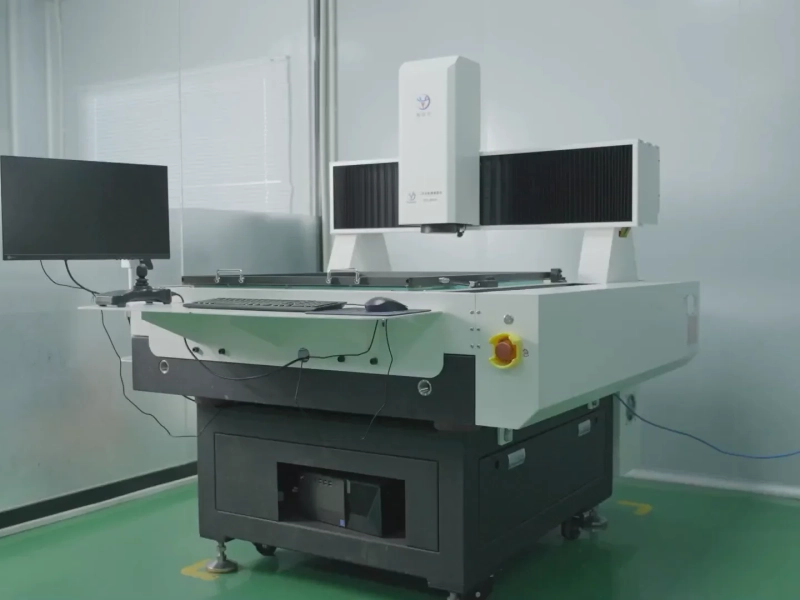
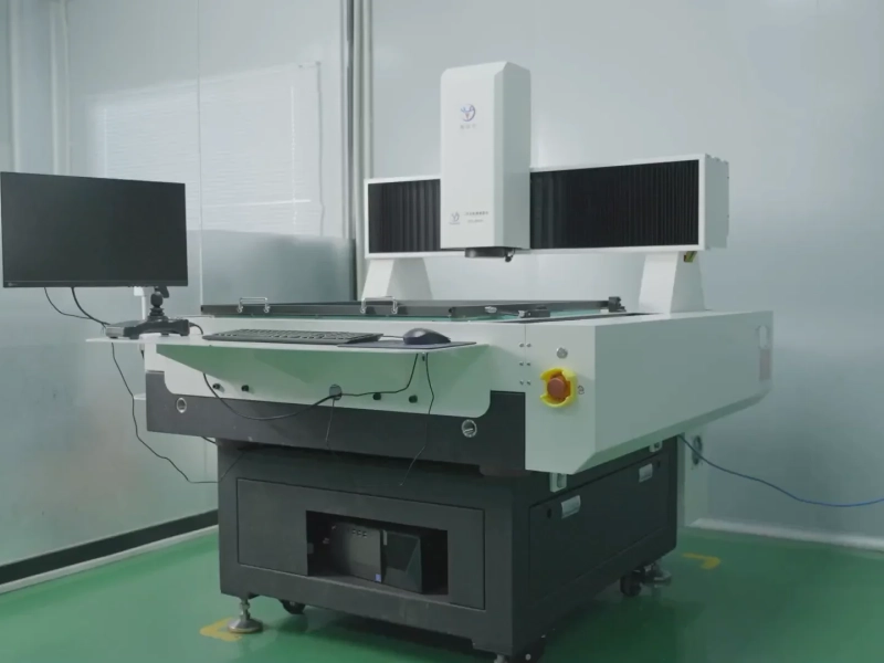
In HDI PCB manufacturing, Engineering Queries (EQs) can delay production when stackup details are incomplete or via structures exceed the fabricator’s capabilities.
- EQ Scenario 1: An engineer submits a 2+N+2 stackup with laser-drilled blind vias (L1–L2 and L2–L3) that are perfectly aligned (stacked vias), yet fails to specify whether copper-filled vias (VIPPO—Via-in-Pad Plated Over) are required.
- EQ Scenario 2: The aspect ratio of a blind via exceeds 1:1, this leads to ineffective electroless copper plating, then forces the factory to issue an EQ to request a change in dielectric thickness.
Reviewing HDI PCB stackup manufacturability before releasing files helps reduce avoidable engineering queries and the risk of rework during sequential fabrication.
3 Core HDI Stackup Manufacturability Rules Every Designer Must Follow
1. Design for Manufacturability of HDI PCB Microvia Structures
The microvia design choices directly affect manufacturing yield and long-term reliability of the board.
- Laser-drilled Blind Vias: Common diameters are 0.075-0.10mm. To ensure solid copper plating, keep your blind microvia aspect ratio within 0.8:1, the maximum limit should be 1:1. Excessive depth increases the risk of plating voids and reduces resistance to cracking under thermal stress. Microvia aspect ratio and laser drilling rules must be checked against the proposed dielectric thickness.
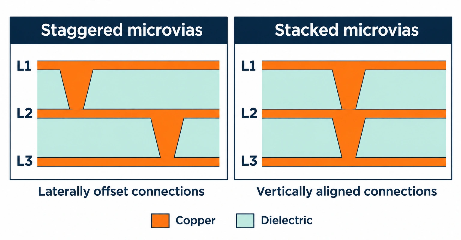
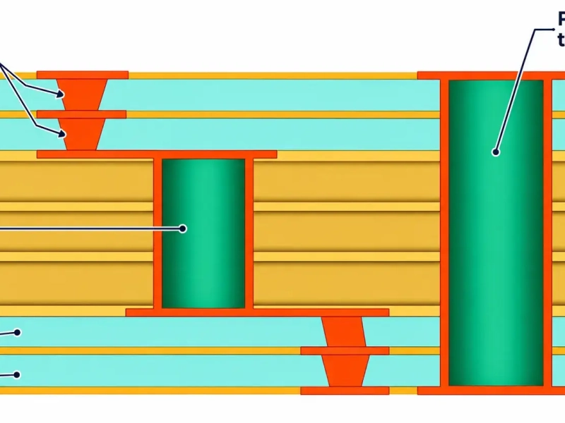
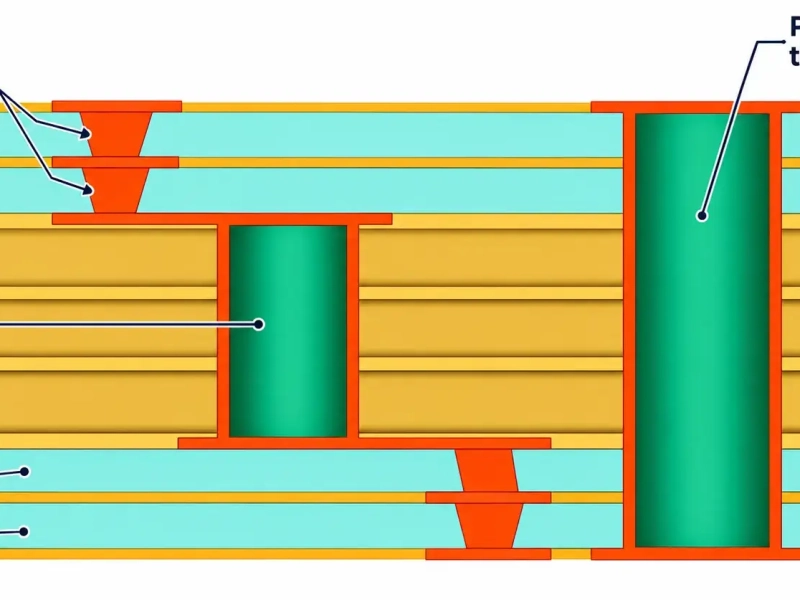
- Staggered Microvias (Highly Recommended): This method offsets the laser holes horizontally between adjacent layers. It is straightforward, highly reliable, offers larger routing channels, and reduces the difficulty of registration compensation. It is usually used for cost-sensitive HDI stackup structures.
- Stacked Microvias (Use with Caution): This vertically stacks laser microvias directly on top of each other. It saves lateral routing space but requires controlled registration, an appropriate lamination sequence, and reliable copper filling. Incomplete filling may lead to voids or trapped process chemicals and create reliability risks. The added processing and inspection requirements can increase cost; compare quotations for the actual structures.
- Via-in-Pad (VIP): This is commonly used in BGA areas with a pitch of 0.5mm or less. VIP structures increase the difficulty of both via filling and assembly soldering, and can increase total manufacturing costs.
- DFM Optimization Strategy: Apply the smallest microvia geometry where the BGA escape routing requires it. Use conventional through-hole designs for the remaining, lower-density regions. This reduces overall manufacturing complexity without compromising total routing density.
For structure-specific reliability evidence, FTG’s Reliability of Stacked Microvia paper (IPC-hosted PDF) compares two-, three-, and four-level stacked microvias positioned on and off buried vias. Its results apply to the tested constructions and conditions, rather than establishing a universal limit for all HDI boards.
2. HDI PCB Materials: Which Properties Affect Manufacturability?
Material selection is a step often overlooked by many engineers. Choosing unsuitable materials can disrupt the structural symmetry of your HDI PCB stackup, which may lead to manufacturing issues such as post-lamination warping and impedance drift.
HDI PCB Material Selection Reference Table: From Standard to Specialized Applications
| Material | Suitable applications | DFM checks | Selection limits |
|---|---|---|---|
| General-purpose FR-4 | Cost-sensitive designs with conventional electrical and thermal requirements | Thin-core and prepreg availability; pressed dielectric thickness; resin filling; laser drilling compatibility | Specify the grade and material construction, rather than only “FR-4.” |
| High-Tg, thermally resistant FR-4 | HDI boards exposed to repeated sequential lamination, reflow, or demanding thermal conditions | Tg, Td, Z-axis expansion, delamination resistance, and validation under the actual lamination and reflow conditions | A higher Tg alone does not establish better overall thermal performance or microvia reliability. |
| Low-loss high-speed laminates | High-speed HDI boards with tight signal-loss budgets | Dk/Df at the target frequency; dielectric thickness and copper foil options; lamination, drilling, and desmear compatibility | HDI construction alone does not justify upgrading to a low-loss material. |
| BT resin-based materials | IC package substrates and structures requiring specific thermal expansion and dimensional stability | In-plane and Z-axis expansion; thin-layer processing; dimensional compensation; lamination conditions for the selected grade | Not a default upgrade for an HDI motherboard. Confirm the fabricator's experience with the material. |
| Rigid-board polyimide laminates | High-temperature service or specialized thermal reliability requirements | Baking and moisture control; cure conditions; drilling and desmear compatibility; thermal cycling validation | Different from flexible PI film. It does not automatically offer lower loss, better moisture resistance, or lower cost. |
Check the selected grade’s published data rather than relying on the FR-4 label alone. For example, Isola’s 370HR material information identifies compatibility with HDI technology and multiple reflows, and discusses sequential-lamination performance. This is an example of grade-specific documentation, not a blanket approval for every stackup.
3. HDI Stackup Structures: How to Choose the Build-Up Level?
Determining the Correct HDI Build Type
Never determine your HDI board layer count or build type purely based on a chip's marketing datasheet. Individual parameters may meet the manufacturer's HDI PCB capability limits while their combination remains difficult to manufacture reliably.
| Structure | Construction | BGA pitch reference | Selection condition | Applications | Cost |
|---|---|---|---|---|---|
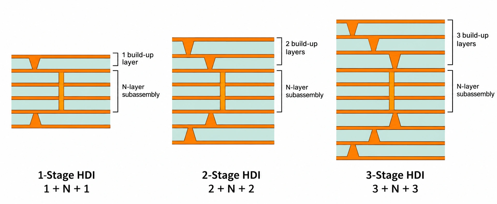
| 1+N+1 | One build-up layer on each side of an N-layer central subassembly | 0.50–0.65 mm | One build-up stage provides enough access for microvia or via-in-pad escape routing | Compact IoT boards, camera modules, small control modules | Baseline: 1.0× |
| 2+N+2 | Two build-up layers per side; staggered or stacked microvias | Approximately 0.40 mm | A single stage provides insufficient layer access or routing channels | High-density SSDs, processor modules, compact communication modules | Higher than one-stage HDI; compare quotes under the same conditions |
| 3+N+3 | Three build-up layers per side | Consider at ≤0.35 mm | Two stages cannot meet escape-routing and board-size requirements | High-density mobile devices, compact computing boards | Higher than two-stage HDI; compare quotes under the same conditions |
| Any-layer HDI / ELIC | Microvias between adjacent layers can be combined to form interconnections | Consider for ultra-fine-pitch, high-density designs | Conventional build-up structures restrict the required interconnections | Highly integrated smartphone motherboards, ultra-compact electronics | Usually highest; the difference from three-stage HDI depends on the complete construction |
Note: "N" represents the copper layers within the initial central core plate. Build-up stages do not directly equal the total lamination counts, the central subassembly and buried vias also affect the process sequence. The BGA pitches above are selection references, escape routing still determines the required structure.
For a practical manufacturing example, see KnownPCB’s 12-layer HDI PCB manufacturing case study, which discusses layer registration, fine-line processing, and microsection inspection in a multistage build.
How to Check Symmetrical Copper Distribution of HDI Stackup
To reduce the risk of warpage (bow and twist) during sequential pressing and assembly reflow, prioritize a balanced structure around the board’s midplane. Review any necessary asymmetry with the fabricator. As explained in Eurocircuits’ copper distribution guidance, both layer symmetry and copper distribution affect mechanical stability. Do not judge balance from Signal or GND labels alone.
Let’s use a classic 6-layer HDI stackup (Signal / GND / Signal / PWR / GND / Signal) as a practical review example:
- Pair the copper layers: Compare L1 with L6, L2 with L5, and L3 with L4. If one side needs heavier copper, evaluate with your fabricator.
- Pair the dielectrics: Compare L1–L2 with L5–L6, and L2–L3 with L4–L5. Ensure the material codes, resin system and glass styles match identically from top to bottom.
- Compare the copper patterns: Look closely at the actual distribution of solid copper planes versus sparse signal tracks across paired layers. Even if the copper thickness is uniform, a structure where L3 contains only minimal routing while L4 features a solid copper plane is still considered unbalanced and carries a risk of board warpage.
- Review the impact of changes. After adding copper or changing layer order, recheck reference planes, impedance, and microvia spans. The fabricator should assess panel-rail copper balancing without compromising the intended electrical function.
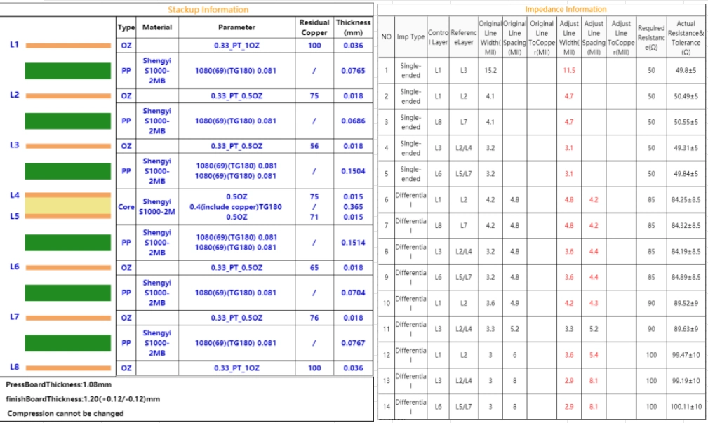
Also check resin filling when specifying dielectric thickness. Isola’s Prepreg Selection: Individual Dielectric Space application note (PDF) explains how copper thickness and etched area affect resin demand and calculated layer spacing. Confirm pressed thickness with the fabricator rather than simply adding nominal prepreg thicknesses.
Essential Engineering Review Checklist to Reduce HDI Fabrication Delays
Before fabrication, submit a consistent data package. Use consistent revisions, layer names, and units throughout.
| Required information | What to include | Purpose of the review |
|---|---|---|
| PCB manufacturing data | Gerber with drill files, or a mutually supported ODB++ or IPC-2581 package. Include all copper and solder mask layers, the outline, necessary markings, and clear layer order. | Reconstruct traces, pads, copper coverage, and board geometry; check completeness and basic manufacturing dimensions. |
| Drill data and layer-pair definitions | Hole coordinates, tool sizes, plated/non-plated status, and start/end layers for each hole group. Supply NC Drill/Excellon with Gerber. Separate drill files need not be duplicated if a readable ODB++ or IPC-2581 package contains all required information. | Confirm hole positions, diameters, and blind/buried connections; prevent missing holes or incorrect layer-pair interpretation. |
| Fabrication drawing and notes | Finished dimensions and tolerances; material grades and substitution rules; surface finish; acceptance standards and revisions; testing and reports. Define copper filling, resin plugging, cap plating, and flatness. Add cross-sections for complex vias and special assembly thermal or reliability requirements. | State process intent and acceptance requirements that the manufacturing data does not fully describe. |
| Stackup and controlled impedance | Layer order; core and prepreg construction; pressed dielectric thicknesses; base and finished copper thickness; overall thickness and tolerance. For controlled impedance, specify targets, tolerances, signal/reference layers, trace widths, differential spacing, and permitted adjustments. | Assess stackup balance, resin filling, microvia aspect ratio, and impedance together; agree on a manufacturable construction and adjustment range. |
| README and revision index | Project and board identifiers; file list and revisions; units; quantity; delivery date; contact. Record approved changes, open questions, and revision relationships between files. | Keep quotation and production based on the same controlled data; reduce revision conflicts and repeated questions. |
FAQs
Do More HDI Layers Always Increase Routing Density?
No. Routing density depends on layer count, microvia structures, trace width and spacing, and BGA escape techniques. Additional layers provide space, but the design may not be able to use all of it effectively.
Blind Vias, Buried Vias, and Microvias—What Is the Difference?
Blind vias connect an outer layer to an inner layer. Buried vias connect inner layers without reaching the board surface. Microvias are typically laser-drilled interconnections. They may be external blind vias or become internal connections after subsequent build-up.
Does a Successful HDI PCB Prototype Build Prove Production Readiness?
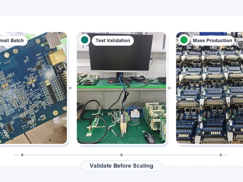
No. Prototype success simply proves that a small batch of boards met the nominal performance window. Mass production requires validating long-term manufacturing stability across high-volume variables.
How Much More Does HDI PCB Cost Than Conventional PCB?
There is no universal multiplier. At similar dimensions, layer counts, and quantities, laser drilling, via filling, and sequential build-up generally add cost. Obtain a quotation for the actual stackup and via construction.
How to Evaluate an HDI PCB Manufacturer?
Check production capability for the proposed build-up, via structures, and material combination. Minimum hole diameter alone is insufficient. Look for pre-production stackup review, specific modification proposals, and agreed quality-verification records.
When evaluating a supplier, compare the proposed stackup and via structure against its published process capabilities. KnownPCB’s HDI PCB manufacturing capabilities provide a starting point for that review; confirm the complete material and geometry combination with the engineering team before release.