
Get A Quote
CN
Blog & Design Guide

A PCB laminate is a bonded material used to form the board's insulating structure, often supplied with copper foil. In a conventional glass-reinforced epoxy multilayer board, a core is a cured laminate used within the stack, while prepreg is partially cured resin and reinforcement that bonds the construction during pressing. Their material states and jobs differ even when they use a related resin system.
That difference affects the fabrication drawing. A core can carry an inner copper pattern before the full board is assembled. Prepreg provides a bonding interval whose final condition is established during lamination. Specify the construction in terms of those roles, then identify the material grade and required cured dimensions.
On this page
The terms laminate, copper-clad laminate and core are related, but they are not interchangeable in every sentence. Laminate names a bonded material. Copper-clad laminate identifies a product supplied with copper on one or both sides. Core describes how a cured piece is used in a particular PCB construction.
Prepreg describes material before its final cure in the board press cycle. For the conventional epoxy construction discussed here, its resin is partially cured and carried by reinforcement. Calling it simply another finished laminate hides the flow and bonding work it still has to perform.
Altium's stackup construction explanation describes the roles of copper foil, prepreg and cured laminate in foil-based multilayer fabrication. Use those roles when comparing a supplier's material description with the layers shown on a fabrication drawing.
A copper-clad core provides a cured dielectric with copper available for patterning. In a common foil-based multilayer build, the manufacturer images and etches the copper on the core before bonding additional material around it. The resulting inner circuitry is already attached to a rigid material when it enters the full-board layup.
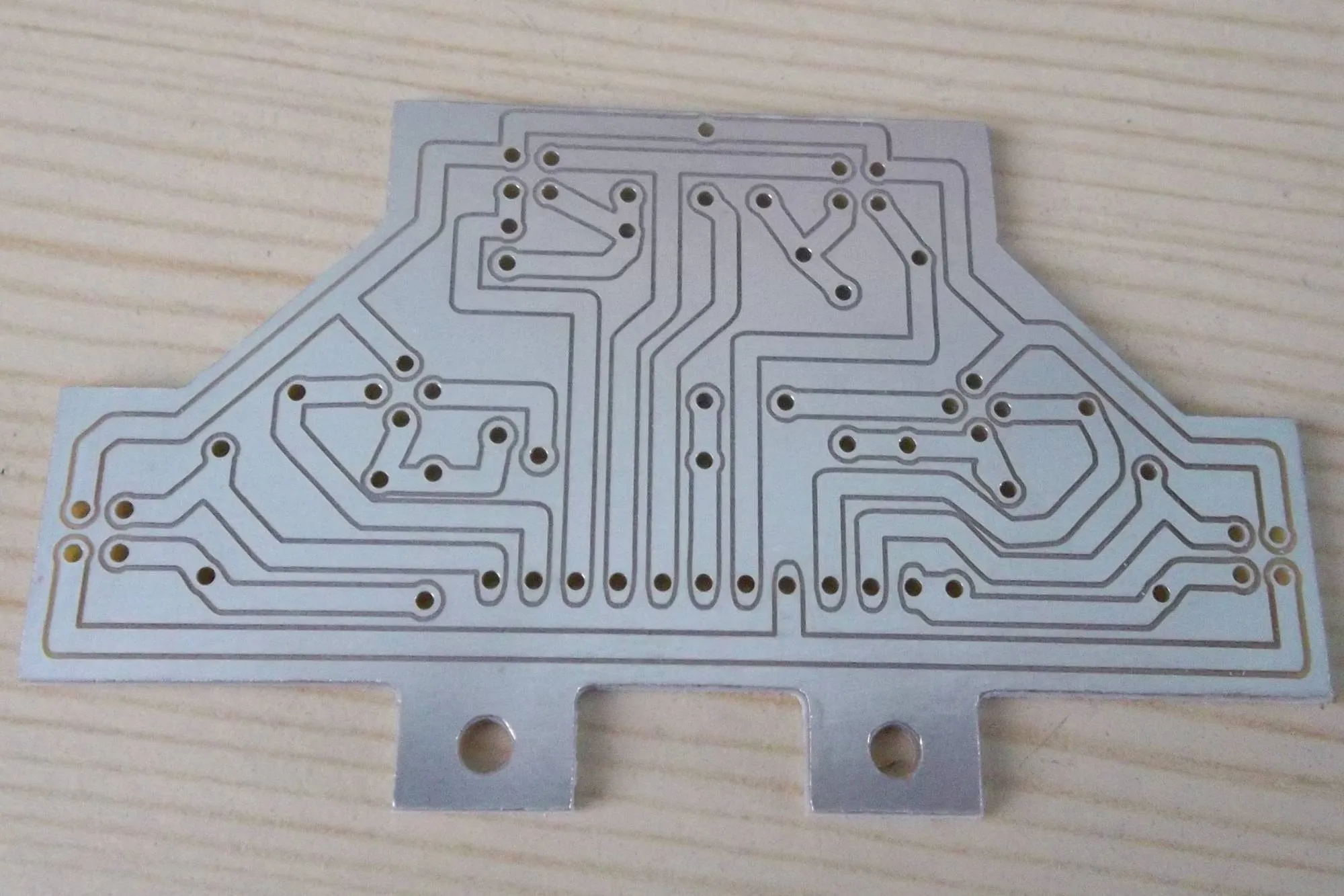
PCB milled from copper-clad board, by Stephen Pithouse, shared under CC BY-SA 3.0; original file.
The core thickness therefore matters both as a material dimension and as a dielectric interval between its copper surfaces. State whether a quoted material thickness includes copper or refers to dielectric alone. A table that mixes those conventions can double-count the foil or omit it from the board-thickness total.
Do not infer the core material from the colour of a finished board. Solder mask, surface finish and photography can obscure the underlying material. Use the released grade, construction and traceable material information for that identification. A board photo can show features and edges, but it is not a substitute for the stackup definition.
During the appropriate press cycle, the resin in a conventional epoxy prepreg softens and flows before further curing. It fills spaces around adjacent copper features and bonds the neighbouring parts of the construction. The process must leave the required dielectric separation while avoiding unfilled regions.
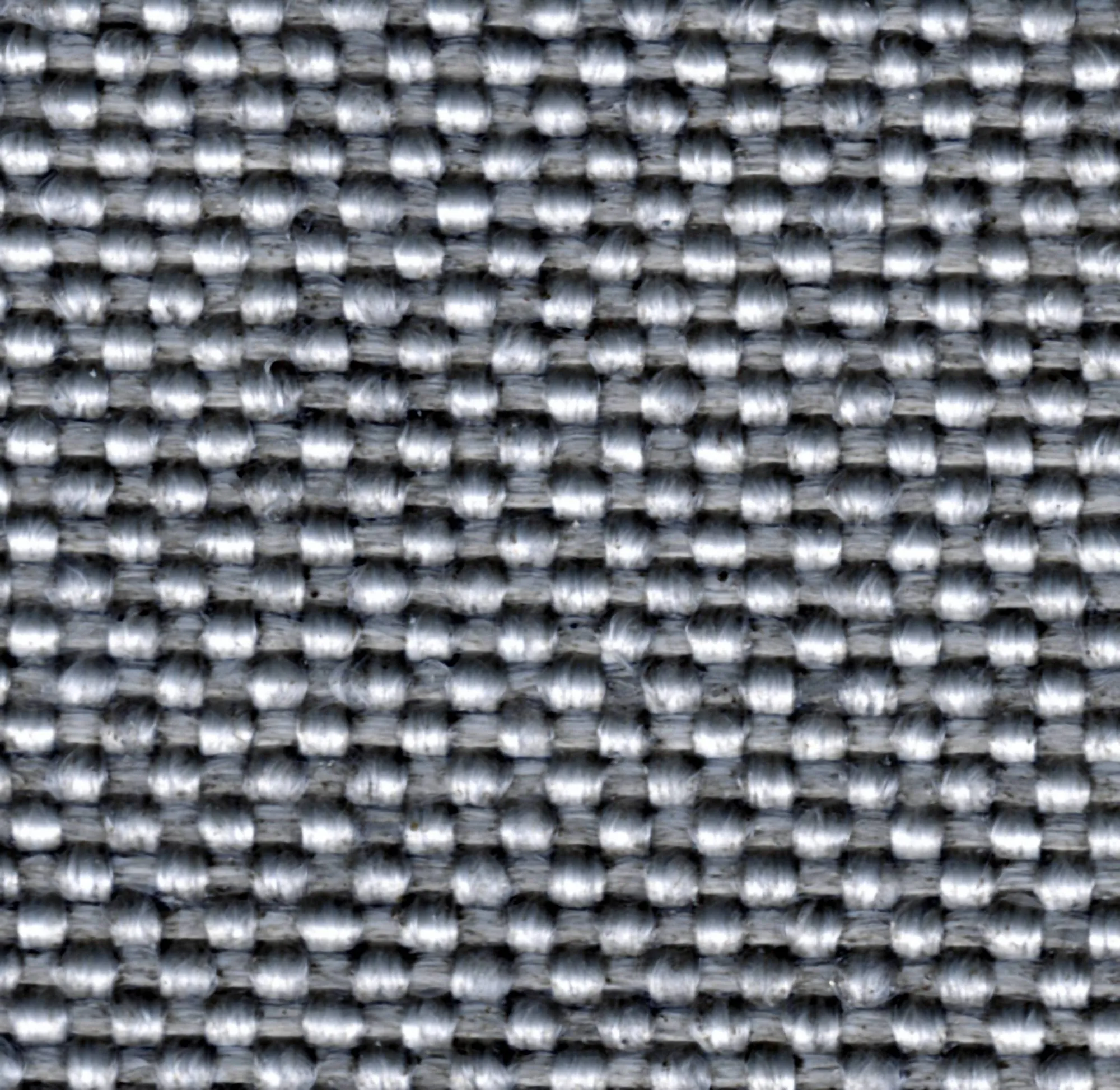
Dry woven fibreglass fabric (1100 g/m²), by Achim Hering, shared under CC BY 3.0; original file. The image shows dry reinforcement fabric, not prepreg.
The reinforcement and the resin serve different roles. Glass cloth provides reinforcement; the resin provides the matrix and bonding material. Dry glass cloth by itself is not prepreg. A material photo should identify which state it actually shows rather than relying on a similar fabric appearance.
A fully cured core does not perform the same flow function as the partially cured bonding sheet. This is the practical reason the materials are called out separately. Press temperature, pressure and time must suit the selected material system and construction; a cycle from another resin grade cannot be treated as a universal setting.
Prepreg selection also depends on what the resin must fill. Compare a nearly solid copper plane with an etched signal pattern containing larger copper-free regions. Their surrounding geometry presents different filling demands. The manufacturer evaluates resin availability, reinforcement and the copper pattern together when establishing the pressed construction.
A four-layer PCB does not need four cores. In one conventional foil-based arrangement, a double-sided core contributes the two inner copper layers. Separate copper foil on the two outside surfaces contributes the other two layers, with prepreg bonding those outer foils to the patterned core.
| Component in this four-layer example | Contribution | What the drawing must distinguish |
|---|---|---|
| One double-sided copper-clad core | Two inner copper layers and their cured dielectric interval | Core dielectric thickness versus a copper-inclusive material dimension |
| Prepreg on each side of the patterned core | Bonding and dielectric intervals | Material construction, ply information and required cured spacing |
| Two outer copper foils | The two outside copper layers | Starting foil and subsequent finished-copper requirements |
The table counts copper layers, not individual prepreg sheets. A bonding interval can use more than one ply of prepreg if required by the approved construction. Conversely, another fabrication approach can arrange cured pieces differently. Identify the actual arrangement rather than assuming every board of a given layer count uses this example.
Altium's core and prepreg arrangement overview describes both typical arrangements and variations. The useful handoff names the dielectric intervals and copper layers separately, so the fabricator can review how the material components satisfy the requested stack.
A prepreg designation is not a complete statement of the resulting board. Record the grade and construction data that control its intended use, including relevant reinforcement and resin-content information. Similar-looking sheets can have different material properties and pressed behaviour.
Clarify the basis of resin content when comparing data. A percentage defined by weight is not automatically a volume fraction, and neither is a direct measurement of the final dielectric interval. Keep the manufacturer's definitions with the material record rather than converting a familiar percentage into an assumed pressed thickness.
The copper pattern adds another constraint. More resin may be needed to fill a region with extensive etched-away copper than a region that retains copper across much of the area. Increasing resin availability is not an instruction to select an arbitrary thicker sheet: the resulting electrical spacing and total thickness must still satisfy the approved stackup.
If a material substitution is proposed, compare the compatible core and bonding materials as a construction. Approval of one core name alone does not establish that any prepreg carrying the same broad FR4 label can replace the original bonding material.
The released stackup should identify where each core and bonding interval sits, what copper belongs to its surfaces, and which dimensions apply after pressing. Distinguish those finished dimensions from the material inputs used to reach them. This makes a production review more useful than a list of purchasing names without layer locations.
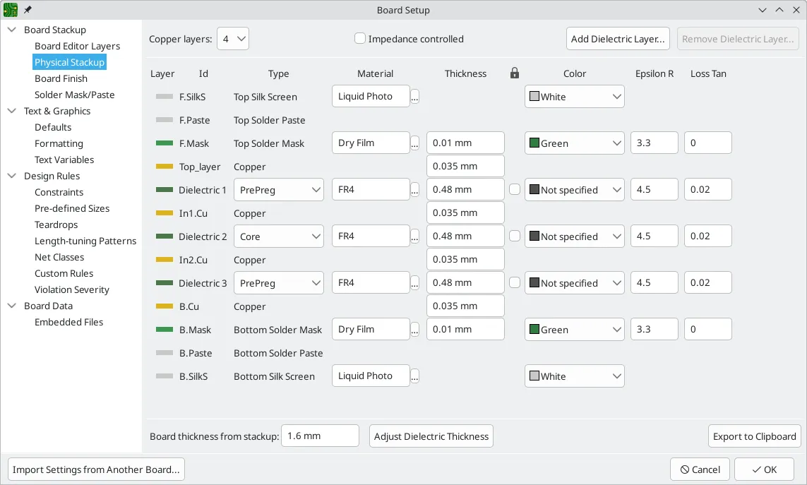
Stackup material fields from the KiCad PCB Editor manual, licensed CC BY 3.0. The example settings are not a KnownPCB stackup.
Open the full-size core and prepreg field screenshot to read its entries.
Where impedance depends on a dielectric interval, identify that interval directly. A manufacturer may be able to meet an overall board thickness using a different distribution of materials, but that does not preserve the distance from every signal layer to its reference plane. Review the affected electrical construction when accepting a changed layer build.
A cross-section can show the completed copper and dielectric arrangement, while the material and fabrication records establish what was used to build it. Keep those records linked to the same revision. Do not label every visible dielectric band in an unrelated example as a known core or prepreg layer unless its construction is documented.
The existing eight-layer manufacturing article applies these construction questions to a particular layer-count context. For different resin systems within one board, the FR4 and Rogers hybrid-stackup article addresses the additional interface and release decisions.
Submit the core and prepreg requirements with the copper build, cured dielectric intervals and finished board thickness. State any restricted material substitutions and identify the electrical properties or construction details that must be preserved when an alternative is reviewed.
Keep the request tied to a fabricated PCB. KnownPCB's multilayer PCB manufacturing page is the product context for reviewing these material callouts, rather than a catalogue for purchasing raw laminate sheets. Use the KnownPCB contact page to discuss the released construction and resolve material or thickness conflicts before the board is put into production.
October/27/2026PCB Differential Pair Skew: Convert Time to Length

September/06/2026High Current PCB Design: Current Paths, Copper, Vias & Thermal Limits
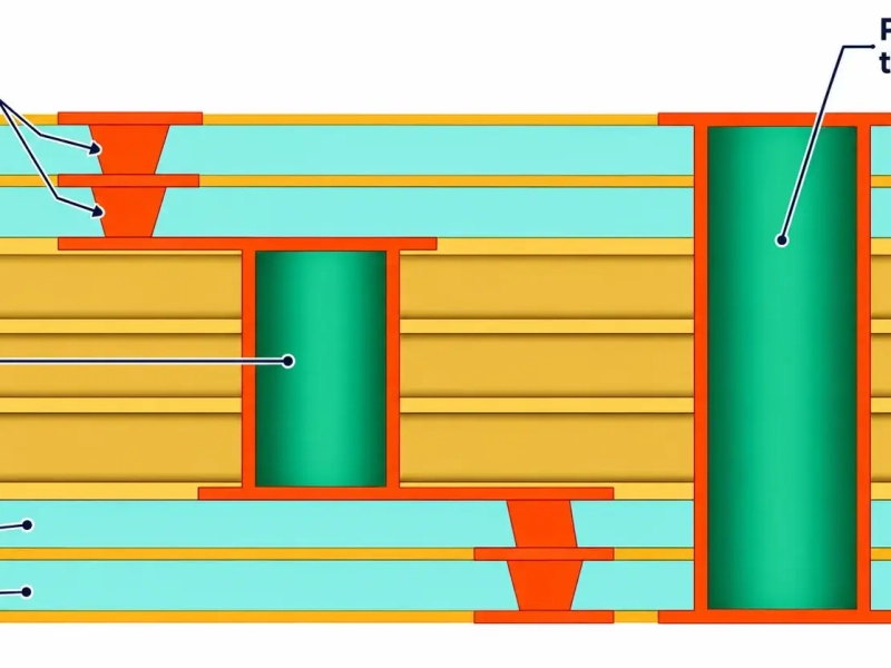
November/05/2026Standard PCB Thickness: Finished Board vs Dielectric
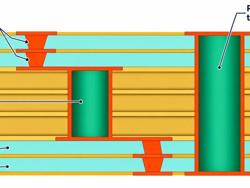
November/05/20266-Layer PCB Stackup: Routing and Reference Planes
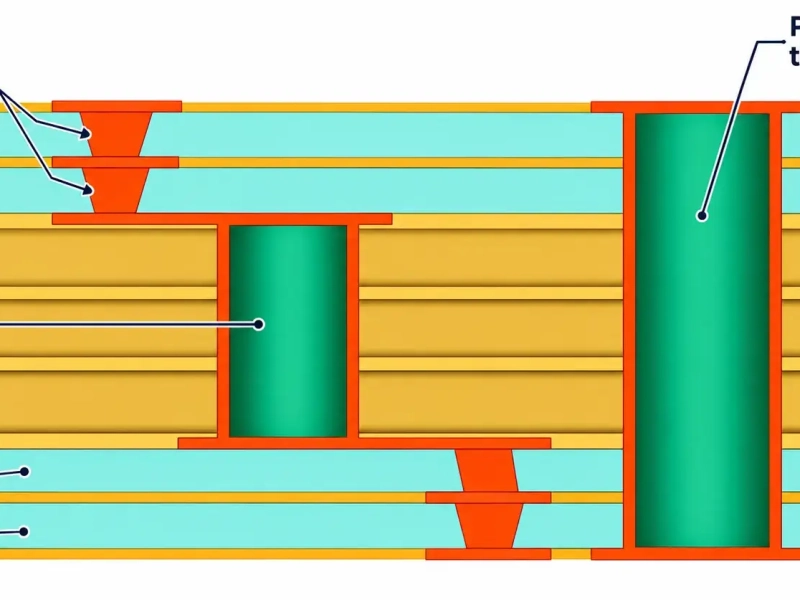
November/03/2026HDI PCB Manufacturers in China: Comparison & 5 Key Checks
Proven by 7 industries, 4000+ customer projects
|
Please contact us at sales@knownpcb.com, ask for engineering support here or use the form below to reach out to KnownPCB |
Request a Manufacturing QuoteInclude your quantity, target delivery date and key requirements. File handling and NDA information. |