
Get A Quote
CN
Blog & Design Guide

Standard PCB thickness describes a commonly offered overall board dimension. It does not specify the distance between a signal trace and its reference plane, the thickness of each core, or the copper on a conductor. A useful order states the finished thickness, its tolerance and the measurement basis, then supplies the layer construction needed for the electrical design.
This distinction matters when the board must fit a connector, enclosure or press-fit feature while also meeting an impedance requirement. The mechanical team needs a total dimension. The electrical team needs particular dielectric intervals. Those requirements must be satisfied by the same released stackup.
On this page
A 1.6 mm board is a familiar purchasing description, and 62 mil or approximately 1.57 mm appears in many stackup discussions. These labels are close, but their exact numerical values differ. Use one controlling unit and tolerance on the fabrication drawing rather than treating every familiar label as an exact equivalent.
| Label or dimension | Exact arithmetic using 1 inch = 25.4 mm | Drawing implication |
|---|---|---|
| 62 mil | 0.062 × 25.4 = 1.5748 mm | A nominal 1.57 mm label may be a rounded description. |
| 1/16 inch | 25.4 / 16 = 1.5875 mm | It is not exactly 62 mil or exactly 1.6 mm. |
| 1.60 mm | 1.60 / 0.0254 = approximately 62.99 mil | Use the specified metric dimension if it controls the design. |
The differences are small enough to be hidden by some tolerance windows, but whether they are acceptable is a drawing decision. For example, an assembly designed around a connector's board-thickness range needs to use that connector's actual fit requirement. A familiar nominal PCB label is not evidence that the finished edge will fit.
Altium's board-thickness discussion describes common and nonstandard constructions and emphasizes selecting a stackup that can achieve the required total dimension. Its listed examples are not a universal menu for every fabricator. Confirm the construction offered for the particular board rather than ordering an unspecified "standard" thickness.
Separate a laminate or core purchase dimension from the thickness of a finished bare board. The completed stack contains several dielectric intervals and copper layers. Outer copper processing and the surfaces at the measurement location also matter to the final dimensional definition.

Outside, inside, and depth micrometers; public-domain image by Splarka via Wikimedia Commons.
Specify whether the controlling measurement is taken over solder mask, over an exposed copper feature, or at a defined board-edge location. Identify any local buildup that should be excluded or separately controlled. Measurements at different surface features can describe different distances even on the same physical board.
A core supplier's nominal thickness also needs a clear basis. Some material descriptions refer to the dielectric while others describe a copper-clad product with its foil. Do not add copper a second time if it is already included in a purchased-material dimension. Equally, do not omit copper when summing values that describe dielectric alone.
Prepreg requires a different distinction: the incoming sheet specification is an input to pressing, while the cured bond-line thickness belongs to the resulting stackup. Resin fills the surrounding copper pattern and the material cures during lamination. Confirm the fabricator's resulting construction rather than substituting an incoming sheet measurement for every cured dielectric interval.
Record the measurement method and locations when the tolerance is important to fit. A single value without its location and surface basis is difficult to compare with another inspection result. For a local mechanical feature such as a card edge, the drawing may need a separate requirement from the nominal dimension of the rest of the board.
The total dimension is a thickness budget. On a consistent measurement basis, add the dielectric contributions, the copper contributions and any surface layers included in the finished requirement. Use finished values where processing changes the dimension, and keep every term in the same unit.
Total thickness = sum of dielectric intervals + sum of copper layers + included surface contributions
Consider an illustrative six-copper-layer budget targeting 1.60 mm, with each finished copper layer taken as 35 micrometres. The copper contribution is 6 × 0.035 = 0.210 mm. If this simplified budget excludes mask and finish, 1.60 − 0.210 = 1.390 mm remains for the dielectric intervals. That remaining total must be distributed among the actual core and bonding intervals; it is not the thickness of each interval.
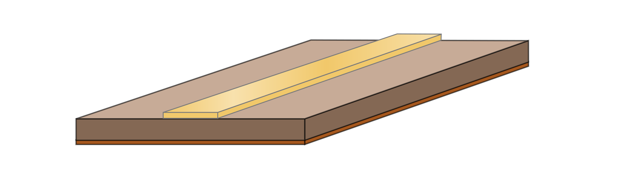
Microstrip structure diagram by Spinningspark, shared under CC BY-SA 3.0; original file.
If two of those intervals are assigned 0.10 mm and 0.20 mm, their combined contribution is 0.30 mm. The other dielectric intervals must then account for 1.090 mm under the same simplified basis. The arithmetic checks whether the proposed terms fit the total, but it does not establish that the selected material combination presses to those dimensions.
This is also why two 1.60 mm boards can need different controlled trace geometry. A signal layer 0.10 mm from its reference plane has a different local field structure from one 0.20 mm away. Making another part of the stack thinner can preserve the total board thickness without preserving that signal-to-plane distance.
Altium's total-thickness and layer-stack explanation separates board, dielectric and copper thickness. Use that separation in the review: first reconcile the mechanical total, then verify each electrically important interval. Do not average all the dielectric layers and use that average as an impedance input.
The existing PCB copper-thickness article addresses copper weight and conductor dimensions. Keep that copper requirement distinct from the finished board dimension. Likewise, the eight-layer stackup article concerns layer allocation; choosing a layer count does not by itself fix the board thickness.
A drawing note should name the finished thickness, the acceptance tolerance, the controlling unit and the agreed measurement basis. For an example requirement of 1.60 mm ±0.10 mm, the acceptance window is 1.50 to 1.70 mm at the specified location and stage. This states the requested window; the fabricator must still review whether the proposed stack can meet it.
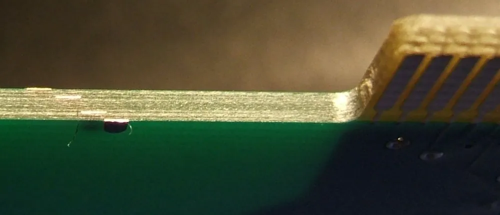
Four-layer PCB edge photograph by Sieobserver / Christoph Kappel, shared under CC BY-SA 3.0; original file.
Cross-check that note against the stackup table and the mechanical drawing. If the stackup total differs from the dimension note, resolve which construction controls before production. Do not let one document retain an old nominal value after another document changes the materials or layer build.
A thickness change also affects holes and interfaces. Check whether it changes the drilled length of a through hole, the depth of a controlled-depth operation, connector engagement or clearance to the enclosure. A backdrill depth referenced from a finished surface must be reviewed against the revised layer positions, rather than copied unchanged from the previous board.
For thin or thick alternatives, request a manufacturable construction using the available materials and required copper distribution. Do not select the total dimension in isolation and assume the fabricator can distribute the remaining dielectric in any requested combination. Local electrical spacing, hole geometry and mechanical fit can impose different constraints on the same stack.
Include the released layer table, finished copper requirements, dimensional note and any location-specific fit requirement when discussing multilayer PCB manufacturing. If the total and the critical dielectric intervals cannot both be satisfied, identify which design requirement may change and obtain approval before fabrication. Send the requirements through the KnownPCB contact page so the review concerns the actual board construction rather than an ambiguous standard-thickness label.

October/10/2026DC-DC Converter PCB Layout: Paths, Thermal Vias and Noise

October/14/2026How to Choose a PCB Manufacturer: Verify the Evidence

October/09/2026Single-Sided PCB Routing: Jumpers, Return Paths, and Width
July/03/2026Single Sided PCB Board: How to Design and Purchase
February/25/2026High-Frequency PCB Performance: Low Dk/Df, Controlled Impedance and Low Signal Loss
Proven by 7 industries, 4000+ customer projects
|
Please contact us at sales@knownpcb.com, ask for engineering support here or use the form below to reach out to KnownPCB |
Request a Manufacturing QuoteInclude your quantity, target delivery date and key requirements. File handling and NDA information. |