
The right choice between flying-probe and fixture-based PCB testing depends on when the test must run, how often the design will change, and how the test points can be reached. Flying probes move between selected copper points without a dedicated bed-of-nails plate. A fixture brings an arranged set of spring probes to corresponding points in one loading operation. For a bare-board open-and-short check, both can test connectivity against released net data. The test method, accessible points, and the report scope should be agreed before the first lot is released.
Define the bare-board test · Compare the two methods · Design for test access · Request a useful report
Fast selection
When the design is changing or the first article needs testing, ask whether flying-probe test is available for the released bare-board netlist. When repeated lots need a shorter test cycle, ask whether a dedicated fixture is practical and what design files, lead time, and inspection records it requires.
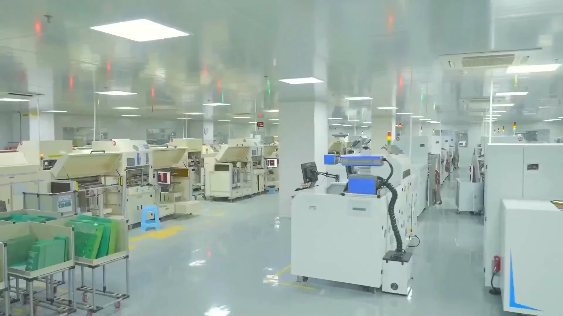
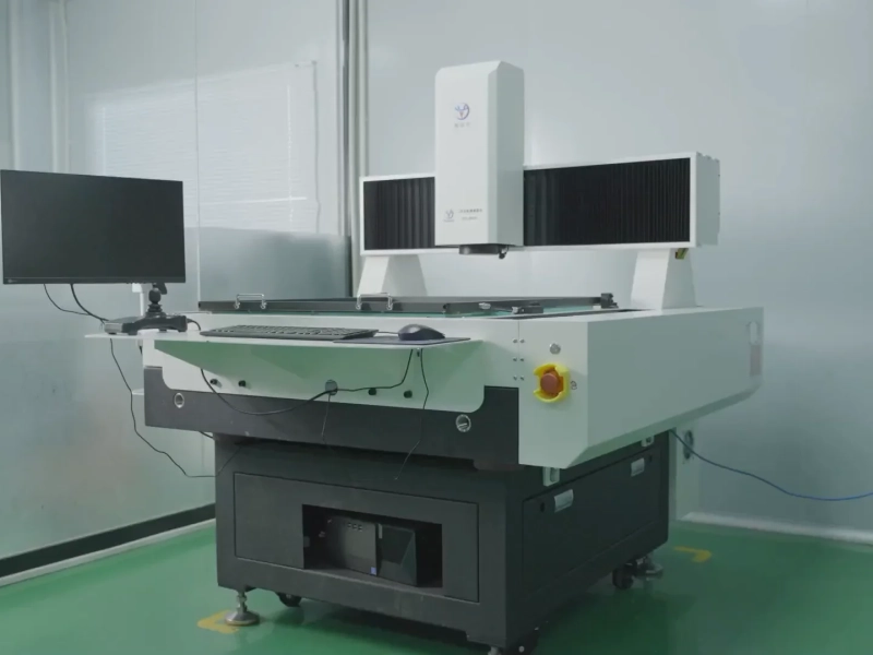
PCB electrical-test equipment on the production floor.
Bare-board electrical testing checks whether specified copper connections remain continuous and whether separate nets avoid unintended contact. The test uses the released data or an agreed netlist to identify the points and pairs under test. It does not evaluate populated components or prove that an assembled circuit performs its intended function.
Altium’s test-point guidance for fabrication testing distinguishes an unpopulated board from an assembled board and describes the use of probe pairs to test a net. That distinction matters when writing the order requirement. State that the request covers bare-board continuity and isolation, name the data revision that defines the nets, and identify any excluded nets or areas where the customer has approved a different treatment.
Before comparing methods, ask what the report will mean by coverage. A board may have accessible copper features that serve as test contact points, yet the tester still needs an agreed netlist and a defined way to process the test. Confirm what the tester will compare and how exceptions will appear in the results.
Flying-probe systems move one or more heads to selected copper locations. A fixture uses aligned spring probes to contact a prepared set of points. These differences affect preparation and repeatability, but they do not by themselves define which electrical nets are tested.
| Decision factor | Flying probe | Dedicated fixture |
|---|---|---|
| How contact is made | Movable probes visit programmed copper locations. | A matching array of probes contacts the board when the fixture is actuated. |
| Preparation to ask about | Programming, access to the selected copper points, and the supplied netlist revision. | Fixture design, tooling or panel alignment, contact map, and any recurring fixture maintenance. |
| When each may suit | Early builds, revisions that may change, or jobs where fixture setup needs review. | Repeated builds where the agreed fixture investment and access plan suit the program. |
| Design questions | Can the probes reach the required copper features without damaging fine or fragile pads? | Do the board, panel, and test-point positions match the proposed fixture layout? |
| Report questions | Does the record identify the programmed revision and unresolved opens or shorts? | Does the record identify the fixture or contact map and the tested panel or lot? |
Do not choose from a volume rule alone. Turnaround and unit economics depend on the supplier’s equipment, fixture charge, board layout, net count, and test plan. Request those details for the actual board so the comparison uses the same revision and coverage assumptions.
KnownPCB’s quality-management overview describes quality controls and inspection services. Use the drawing and netlist when asking which bare-board electrical-test approach can be offered for a specific job.
Flying-probe testing generally uses copper features already present in the design, while a fixture depends on the positions and contact plan agreed for the fixture. Both methods need access to the test locations. Use the finished solder-mask data and the actual panel orientation to identify reachable exposed copper.
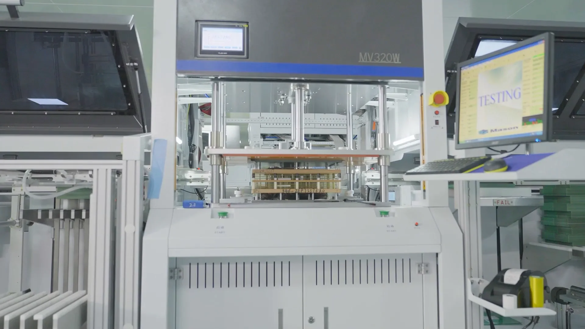
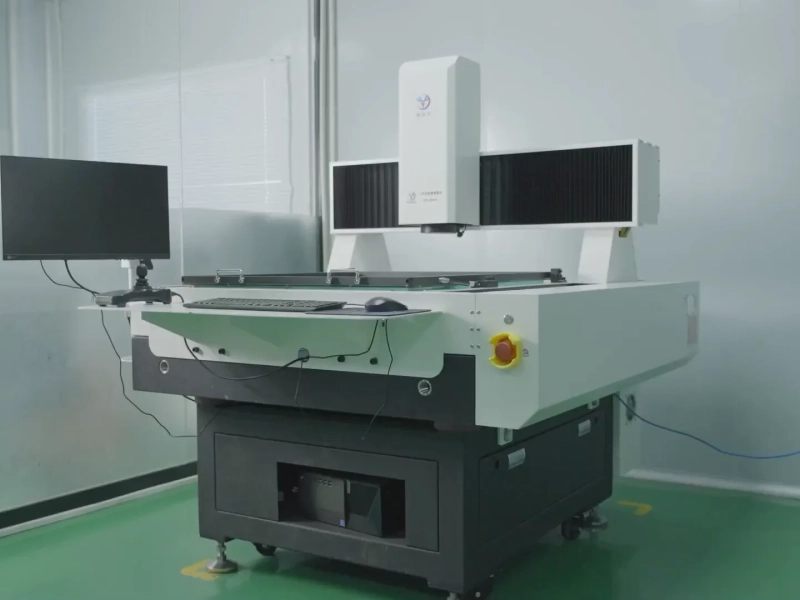
Control screen beside an automated PCB electrical-test station.
If a small pad is difficult to contact, review whether another exposed feature on the same net is suitable. Confirm the location with the fabricator against the final mask openings and the approved test program. The test contact map should identify which side of the panel is accessed and where fixture or probe clearance limits coverage.
Send the final layer and drill data, copper images, outline, netlist, panel plan, and revision together. If the supplier’s chosen test method needs a contact area or panel change, review it against the electrical design before approving the update.
A useful electrical-test record connects the result to the exact files and lot. Ask for the board revision, the netlist or test-data revision, the tested panel or sample identification, the selected method, and the disposition of failed or untested nets. Agree in advance whether the report is a summary or includes per-board results.
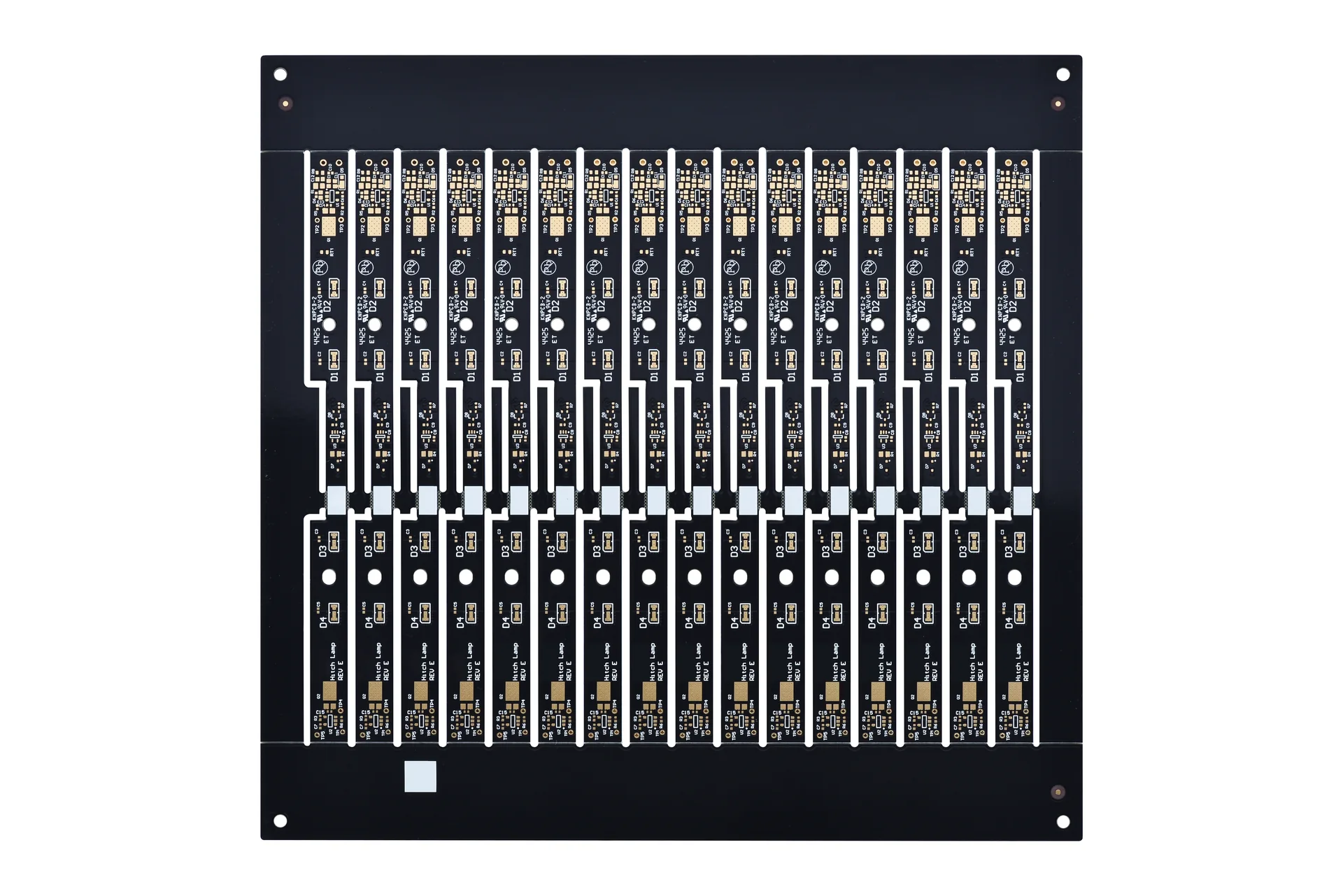
Bare-PCB panel with repeated circuit strips and visible edge contacts.
Read the report against the released data. A reported pass has meaning for the tested connections and stated coverage. It should not be presented as a functional test of an assembled product unless that separate test was actually performed and recorded.
For a project-specific request, send the data package through the KnownPCB contact page and ask the team to confirm the available bare-board test method and report scope.
March/10/2026How 0.2–1.2 mil Solder Mask Thickness Affects 100 Ω Differential Impedance and Insertion Loss
October/09/2026ENIG Black Pad: Inspection and Lot Traceability

April/24/2026Aluminum vs Copper vs Stainless Steel MCPCBs: Thermal Performance, Cost and Applications
March/20/2026Automotive Multi Camera System Demands and Challenges in PCB Process
October/27/2026PCB Copper Roughness: Skin Depth and Conductor Loss