
Choose between V-scoring and tab routing by starting with the board outline and the edge the assembled product needs. V-scoring suits straight shared borders where a continuous scored line can cross the panel. Tab routing suits outlines that need separate milling paths or portions of perimeter to remain uncut. Connector access, component clearance, handling strength, and the required finished edge can rule out either choice. Decide with the board shape visible, then specify how the units remain connected and how the panel separates.
Start with the outline · Check the V-score path · Check the routed tabs · Release edge details
Panel-edge decision
All separation edges are straight and the same cut line is acceptable? Review V-scoring.
Some outlines curve, turn, or need cutouts? Review tab routing.
Both methods fit? Compare edge quality, support during assembly, and whether partial separation is allowed.
Begin with the final outline for every unit and the edge that must meet the enclosure or connector. Identify straight shared borders, internal cutouts, curved portions, and any edge that should remain continuous. A simple panel sketch helps the fabricator see where a common line can cross all units and where the cutter needs to follow a separate perimeter.
Also mark parts near the edge. A connector, component, exposed pad, or fragile structure may need clearance from the V-groove or routed path. Check both sides of the board and the direction from which the panel will be handled. The separation line must leave room for the finished product outline and the planned assembly process.
A V-score forms aligned grooves along the panel line so the repeated boards can separate there after processing. It works best when the edge follows a continuous straight path. Neighboring board edges need to align with that path, and the final edge geometry must allow the scored groove to pass between units.
Check these conditions on the panel drawing:
V-scoring can be economical for repeated straight borders, but it limits the outline that can be formed on the shared edge. A notch or shaped perimeter on that boundary may call for a routed segment or another agreed panel construction. The applicable groove dimensions and product-edge condition must be confirmed for the specified board and process.
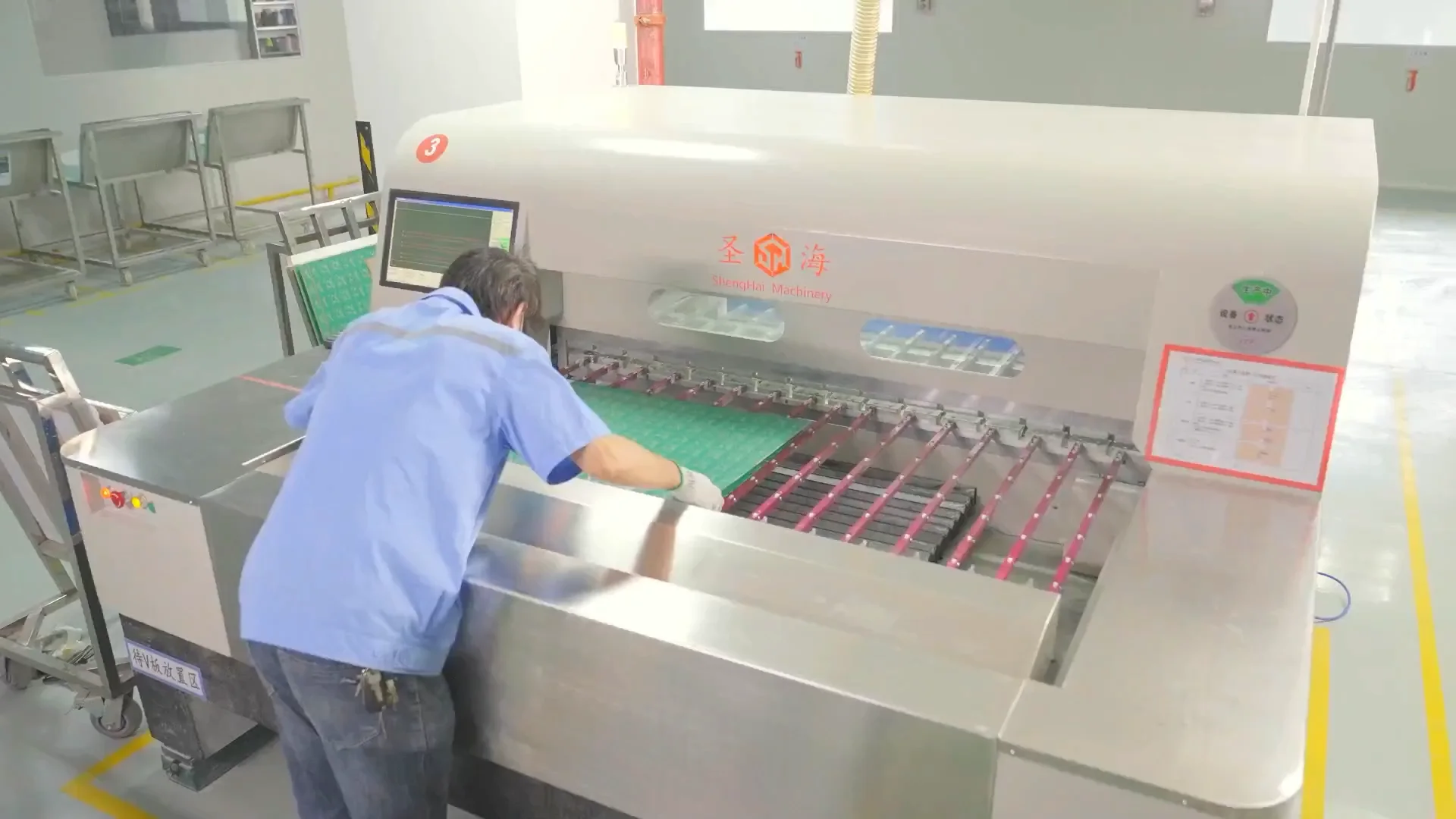
PCB panel being loaded at a V-scoring station.
Tab routing uses a milling path around board outlines while leaving small bridges to hold each unit in the panel. The path can follow shapes that a continuous score cannot cross. Designers may add perforations along the bridges so the parts can be separated with less manual cutting, subject to the fabricator’s tooling and the product’s edge requirements.
Review the drawing in this order:
Small perforations can ease separation, while bridges preserve panel support. Both leave an edge that needs review after the unit is broken from the panel. Discuss possible breakout marks, edge roughness, and board movement with the fabricator when those conditions affect fit or reliability. Do not assume one universal bridge count or perforation pitch. Those details depend on panel dimensions, board thickness, route geometry, and tooling.
Altium’s overview of mouse bites and V-scores describes how the methods separate units from a panel and why the final outline affects the choice.
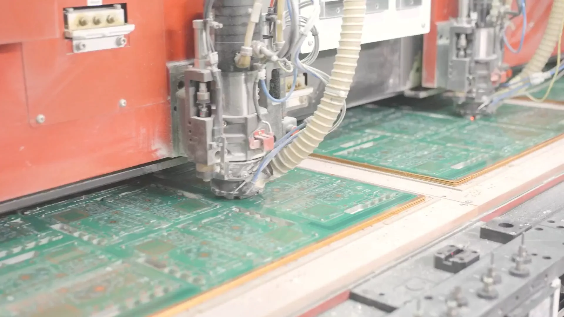
Close view of a CNC router working over a PCB panel.
Include the individual board outline, panel outline, separation features, and any edge condition that matters to the enclosure or connector. Identify which boundaries are scored and which are routed. For tabs, show their locations and any requested perforation pattern. For V-scores, mark the continuous score lines and make sure they align with the intended unit edges.
 Multilayer PCB units held in a larger array with routed separation paths.](/upload/image/20261113/multilayer-pcb-depth-routing-02.webp "[multilayer-pcb-depth-routing-02.webp](/users/mac/desktop/knownpcb/batch-2026-11-11-next8/media/k22/multilayer-pcb-depth-routing-02.webp) multilayer pcb units held in a larger array with routed separation paths.")
Multilayer PCB array with routed outlines between repeated units.
Keep the outline, copper, solder mask, and assembly drawing on the same revision. Ask the fabricator to flag a component or copper feature that conflicts with the proposed cut path before the panel design is released. If the assembly house needs units partly separated or fully separated, state that requirement in the purchase and assembly handoff. For an edge with a tight fit, specify where a residual tab is acceptable and how the finished unit will be checked.
The existing PCB panelization article covers broader panel formats. For mixed-design panels, see the multi-design panelization review. Discuss a prototype or low-volume panel with KnownPCB through the prototype and low-volume PCB service page.
October/28/2026Thermal Via Resistance: Plating, Diameter and Arrays
October/22/2026Telecom PCB Manufacturing: Release the Critical Channel
May/15/2026MOSFETs and SMT Integration
November/13/2026PCB Etch Compensation and Finished Trace Width
November/05/2026HDI Sequential Lamination: Via Layers and Build Order