Get A Quote
CN
Thermal via resistance can be estimated from the copper in the via barrel. The first calculation uses the copper cross-section, the board thickness, and an assumed copper conductivity. It gives an ideal one-dimensional resistance for the barrel alone. It does not give junction-to-ambient resistance or predict the temperature of a complete assembly.
The geometry matters. A plated through via is a hollow copper cylinder, so the conducting area is an annulus. Increasing the plating thickness increases copper area. Increasing board thickness lengthens the heat path. Adding identical vias places ideal barrel paths in parallel, although the real board also has spreading and contact limits.
The examples below use a finished open-hole diameter of 0.30 mm, 25 μm of barrel copper, a 1.6 mm board, and an ideal copper conductivity of 400 W/(m·K). These are illustrative inputs. They are not a KnownPCB process specification, a measurement, or a recommendation for a particular package.
Contents
Thermal resistance is the temperature difference across a defined path divided by the heat flow through that path. It is written in K/W or °C/W. For a simple uniform conductor, R = L/(kA), where L is path length in metres, k is thermal conductivity in W/(m·K), and A is the cross-sectional area carrying heat in square metres.
That equation assumes steady heat flow in one direction through a uniform material. A via barrel can be approximated this way for a first comparison. The calculation leaves out the copper pads, internal planes, spreading into a plane, interface contact, solder, and heat paths through other parts of the board. Those contributions need a separate model or measurement.
For a through-hole example, the via length may be approximated by the board thickness. A blind or buried via uses only its actual plated vertical segment between connected layers. Put that conductive length in L rather than using the full board thickness automatically.
Keep the units visible through the calculation. A millimetre must become 0.001 metres, a square millimetre must become one millionth of a square metre, and the temperature difference is in kelvins or degrees Celsius. A result in K/W means that one watt flowing through the defined path produces that many kelvins of temperature difference in the ideal model.
The resistance of a thermal via also differs from its electrical resistance. The thermal equation uses thermal conductivity and cross-section. An electrical current limit needs electrical resistivity, current distribution, temperature rise, copper quality, and the board's electrical requirements. A thermal via calculation does not set a safe current rating.
A thermal via usually transfers heat from a component pad toward a copper plane or the opposite board surface. TI's thermal design application note discusses vias as part of the path from a device pad through the PCB to a heat sink. Its component, board, and thermal boundary conditions matter. Do not reuse a package-level result as the resistance of a different barrel or finished assembly.
A photograph of a copper-plated panel helps show the manufacturing environment. It cannot reveal the copper thickness inside a selected barrel or the temperature difference across the via.
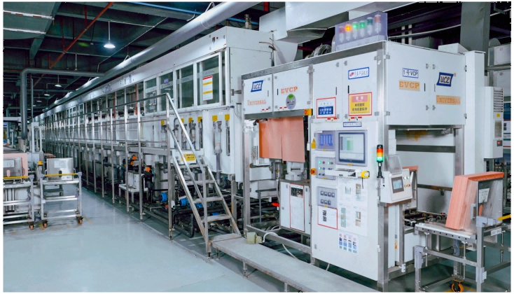
The photograph shows plating equipment. It does not measure the copper in any specific via barrel.
For this article, Dfinished means the open bore diameter after plating. The copper barrel surrounds that opening. If the copper thickness is t, the outer copper diameter is Dout = Dfinished + 2t. The conducting cross-section is the outer circle minus the open hole: A = π/4 × (Dout² − Dfinished²).
Use a drawing that states what the finished hole dimension measures. Some drawing conventions distinguish a drill tool diameter from the finished open bore. Do not insert the drill size into this equation unless it is the dimension that actually defines the opening after plating. The term t is the copper thickness on the via wall, not the surface copper weight in ounces.
Worked example 1 uses a 0.30 mm finished open bore and 25 μm of barrel plating. Convert the plating thickness to 0.025 mm. The outer copper diameter is 0.30 + 2 × 0.025 = 0.35 mm. The annulus area is π/4 × (0.35² − 0.30²) = 0.025525 mm², or 2.5525 × 10⁻⁸ m².
Now use a 1.6 mm board and k = 400 W/(m·K). The resistance is 0.0016 m ÷ (400 × 2.5525 × 10⁻⁸ m²) = 156.7 K/W for one ideal barrel. The value is high because the copper annulus has a small cross-section. It applies to that vertical copper path only.
The conductivity input is an approximation. NIST's OFHC copper property data give a temperature-dependent fit by residual-resistivity ratio. The RRR 100 fit is about 396.3 W/(m·K) at 300 K, which rounds to 400 for this example. That high-purity reference does not certify the conductivity of an electrodeposited via barrel. Grain structure, impurities, temperature, and plating process can change the actual value.
The cross-section figure below distinguishes the hollow annulus from a fully copper-filled cylinder. Both examples use the same 0.35 mm outside diameter. The graphic is not to scale.
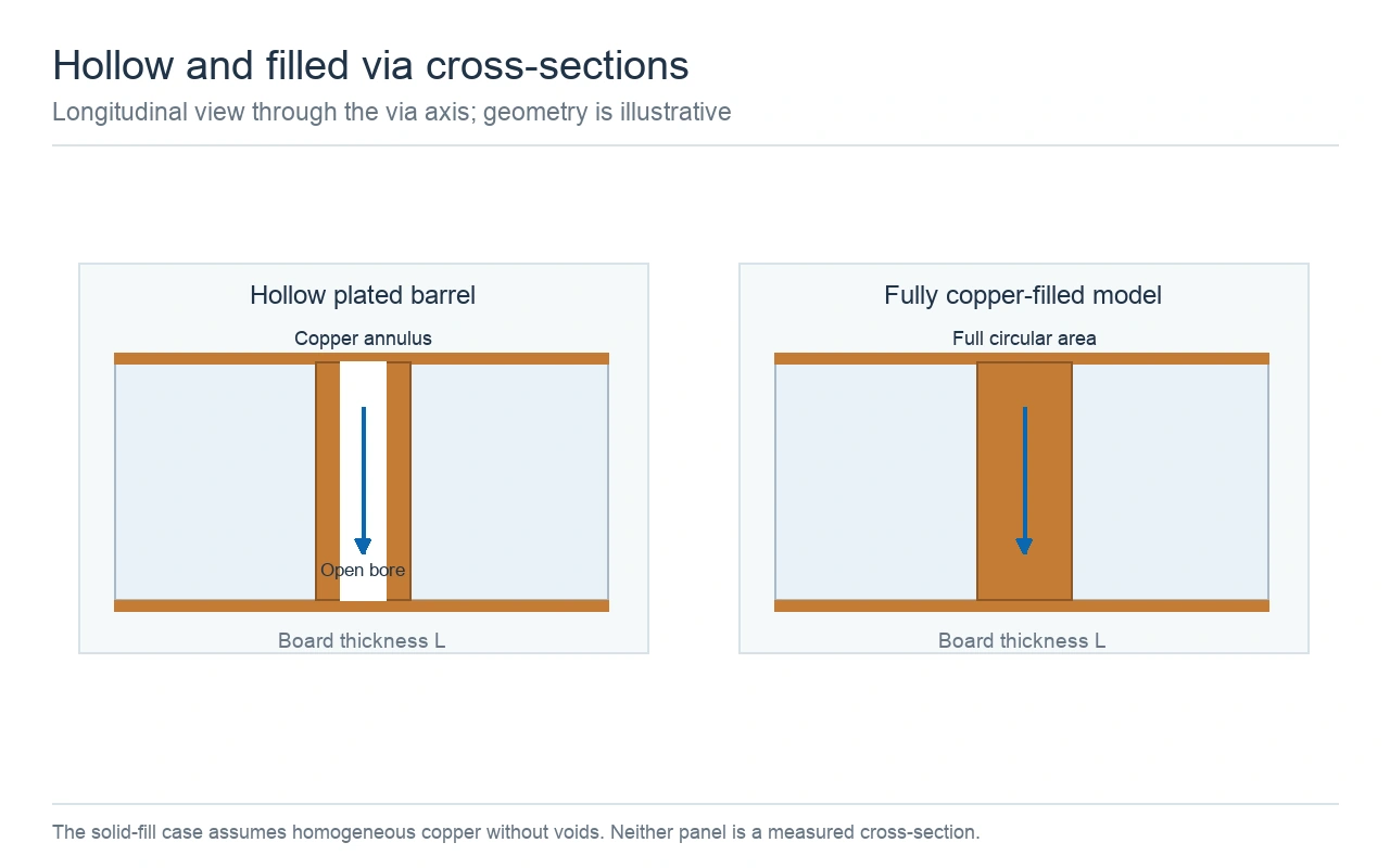
The filled cylinder is an ideal geometric comparison. It does not represent a measured fill or a specific manufacturing result.
At 0.35 mm outside diameter, a solid copper cylinder has an area of 0.096211 mm². With the same 1.6 mm length and 400 W/(m·K), its ideal resistance is 41.6 K/W. Its copper area is about 3.77 times the annulus area. This comparison assumes that the entire fill is homogeneous copper without voids. A filled process may use a different material or contain defects, so the calculation is only a limiting geometry case.
The dimension sketch below marks the open bore, copper wall, and outside diameter used in the equation. It defines the article's geometry convention. A production drawing still needs to state how its finished-hole dimension is measured.
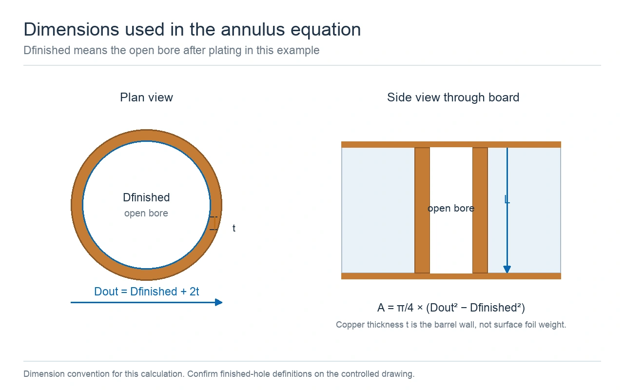
The calculation defines Dfinished as the open bore after plating and Dout as the outside of the copper wall.
With the open bore held at 0.30 mm, thicker barrel copper adds area around the opening. Under the simple model, that lowers barrel resistance. The effect is nonlinear because the copper is an annulus rather than a solid circle. Real plating thickness also varies along the hole and across a panel, so the nominal input should come from the controlled drawing and an agreed inspection method.
Diameter affects both copper area and board layout. With plating held at 25 μm, a larger open bore also increases the outer diameter, so the annulus becomes larger and the ideal resistance falls. That result does not mean the largest possible hole is the best design. It uses more area, may conflict with component pads or routing, and can change solder behavior when the via sits under an exposed pad.
The sensitivity table changes one input at a time. The three plating rows hold the open bore at 0.30 mm. The diameter rows hold plating at 25 μm. The length rows use the 0.30 mm bore and 25 μm plating. All rows use k = 400 W/(m·K), steady one-dimensional heat flow, and ideal uniform copper.
| Changed input | Other geometry | Copper area | Ideal barrel resistance |
|---|---|---|---|
| Plating 15 μm | Open bore 0.30 mm, length 1.6 mm | 0.014844 mm² | 269.47 K/W |
| Plating 25 μm | Open bore 0.30 mm, length 1.6 mm | 0.025525 mm² | 156.71 K/W |
| Plating 35 μm | Open bore 0.30 mm, length 1.6 mm | 0.036835 mm² | 108.59 K/W |
| Open bore 0.20 mm | Plating 25 μm, length 1.6 mm | 0.017671 mm² | 226.35 K/W |
| Open bore 0.30 mm | Plating 25 μm, length 1.6 mm | 0.025525 mm² | 156.71 K/W |
| Open bore 0.40 mm | Plating 25 μm, length 1.6 mm | 0.033379 mm² | 119.83 K/W |
| Board length 0.8 mm | Open bore 0.30 mm, plating 25 μm | 0.025525 mm² | 78.35 K/W |
| Board length 1.6 mm | Open bore 0.30 mm, plating 25 μm | 0.025525 mm² | 156.71 K/W |
| Board length 2.4 mm | Open bore 0.30 mm, plating 25 μm | 0.025525 mm² | 235.06 K/W |
A wider via array can provide parallel heat paths. Worked example 2 takes the 156.71 K/W one-via estimate and divides it by 16 identical vias. The ideal array result is 156.71 ÷ 16 = 9.79 K/W for the barrel paths. The same model gives 39.18 K/W for four vias. This assumes that all vias connect the same two temperature nodes and that each one carries an equal share of heat.
That assumption breaks down when vias share copper planes, sit at different distances from a heat source, or connect through different pad and solder conditions. Heat spreading in the planes can make nearby vias compete for the same region. The real array therefore does not always improve in direct proportion to via count.
TI's PowerPAD thermal design report shows package-specific via patterns and resistance curves for different die areas and two-layer or four-layer boards. It notes a point where adding vias gives diminishing improvement, and it ties the result to the package, exposed-pad soldering, copper planes, and the heat-removal method. Use its guidance for the matching package family, not as a universal via count for every board.
The array chart below shows the mathematical limit Rarray = Rone/N. It uses the worked example for every via and plots no spreading, contact, plane, or package resistance. The curve helps compare barrel count in the ideal model. It is not a thermal simulation of an assembled product.
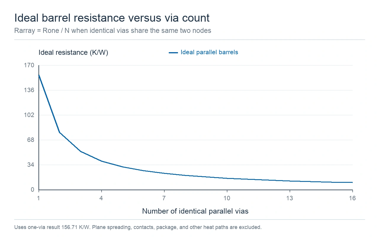
Ideal parallel barrels only, using the article's illustrative inputs. Board spreading and interface resistance are excluded.
A component's heat does not start at the via barrel. It leaves the semiconductor junction through the package, crosses the exposed pad and solder joint, enters the board land, spreads through copper, and then reaches a housing or surrounding air. Every part of that path has a resistance or a heat-flow split.
For a first series estimate, a designer may add the package, solder, pad, via array, plane-spreading, and interface terms when the same heat flows through each segment. Real assemblies often have parallel paths. Heat can move through package leads, top copper, internal layers, an attached heat sink, and air at the same time. A single sum is valid only when the boundaries and heat paths match the model.
The network figure shows a via term inside a larger path. The relative box sizes are symbolic. They do not show a tested resistance split or indicate which term dominates a particular design.
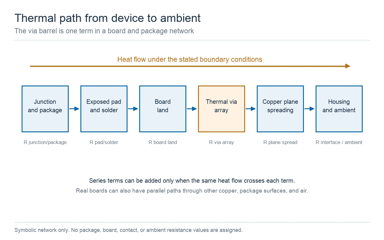
A system model needs temperatures, heat flow, contacts, and parallel paths. The drawing contains no measured values.
A board photo can show where a thermal pad or copper region sits, but it does not expose the buried barrel or the temperature drop across it. Use a drawing for geometry and measurement data for thermal performance.
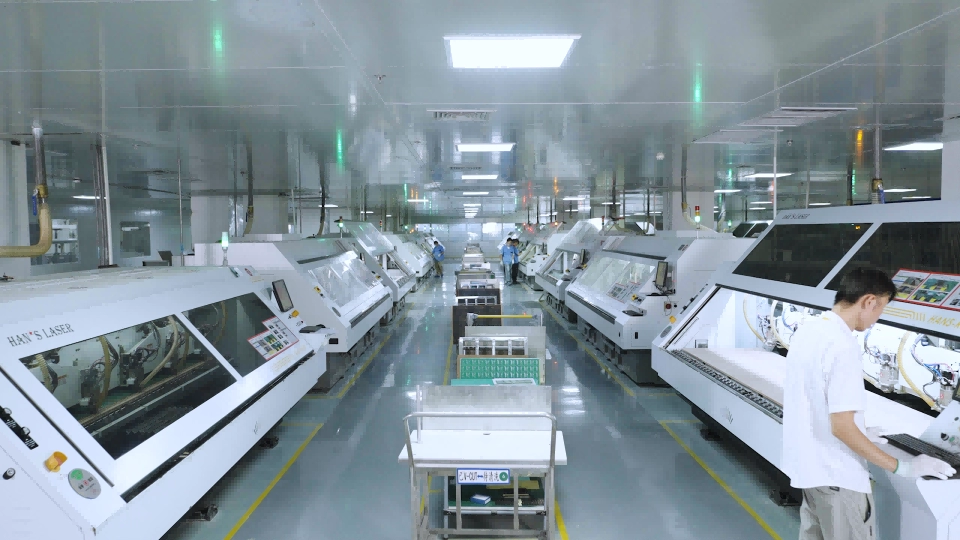
The photograph shows drilling equipment, not a thermal-via cross-section or measured thermal result.
The component's power loss and the chosen temperature boundary also matter. A resistance value alone does not tell you the junction temperature. For a single defined path, ΔT = P × R. Use the heat actually entering that path and the temperature difference between the same two endpoints. Do not combine junction-to-case values with board-to-ambient values unless the component and board paths connect at the specified reference points.
A useful thermal via drawing defines the finished open-hole diameter, barrel copper thickness, board thickness, via count, spacing, connected layers, pad dimensions, and any fill or cap requirement. It should also show whether the via sits inside a component's exposed pad and whether solder can wick through the opening. These details affect assembly as well as heat flow.
The result should state its boundaries. Record the temperature measurement points, heat input, board layer count, plane size, copper thickness, solder condition, housing contact, and airflow. If a supplier report gives one thermal resistance, ask which surfaces the measurement spans and whether it includes the package, board planes, or interface material.
Use the KnownPCB multilayer PCB page for general stackup context, and review the quality management information when defining project records. Send the exact drawing through a manufacturing enquiry if the proposed construction needs review. These pages do not establish a specific thermal-via plating thickness or a guaranteed resistance.
A thermal simulation should use the board stackup and package boundary that will be built. Compare the result with measurements at named points. If the test changes the heat sink, solder coverage, airflow, or clamp pressure, the comparison includes those changes as well as the vias.
Use the barrel equation to screen geometry and explain why plating, length, and count change the ideal result. Then place that term inside a board and package model. The two stages answer different questions, and the second needs the complete thermal path.