
Get A Quote
CN
HDI sequential lamination adds layers in stages so that the required connections can be formed while their target copper is accessible. A buried connection must be processed before later material covers it. A blind microvia reaches the target exposed beneath a thin build-up dielectric. The finished cross-section records where the connections end up, but the fabrication plan must also identify when each connection is made.
Start with the via layer pairs. Then group the layers that can be fabricated together, identify the connections that will become inaccessible, and build outward. That sequence gives engineering a way to discuss an HDI construction without treating a layer-count label as a complete manufacturing instruction.
On this page
List the start and end layer of every distinct hole structure. A note saying "blind and buried vias" leaves the most important information unresolved. A hole from L1 to L2 has a different construction requirement from a hole passing through an inner sub-stack. Use the same final layer names in the layout, stackup, drill information and fabrication drawing.
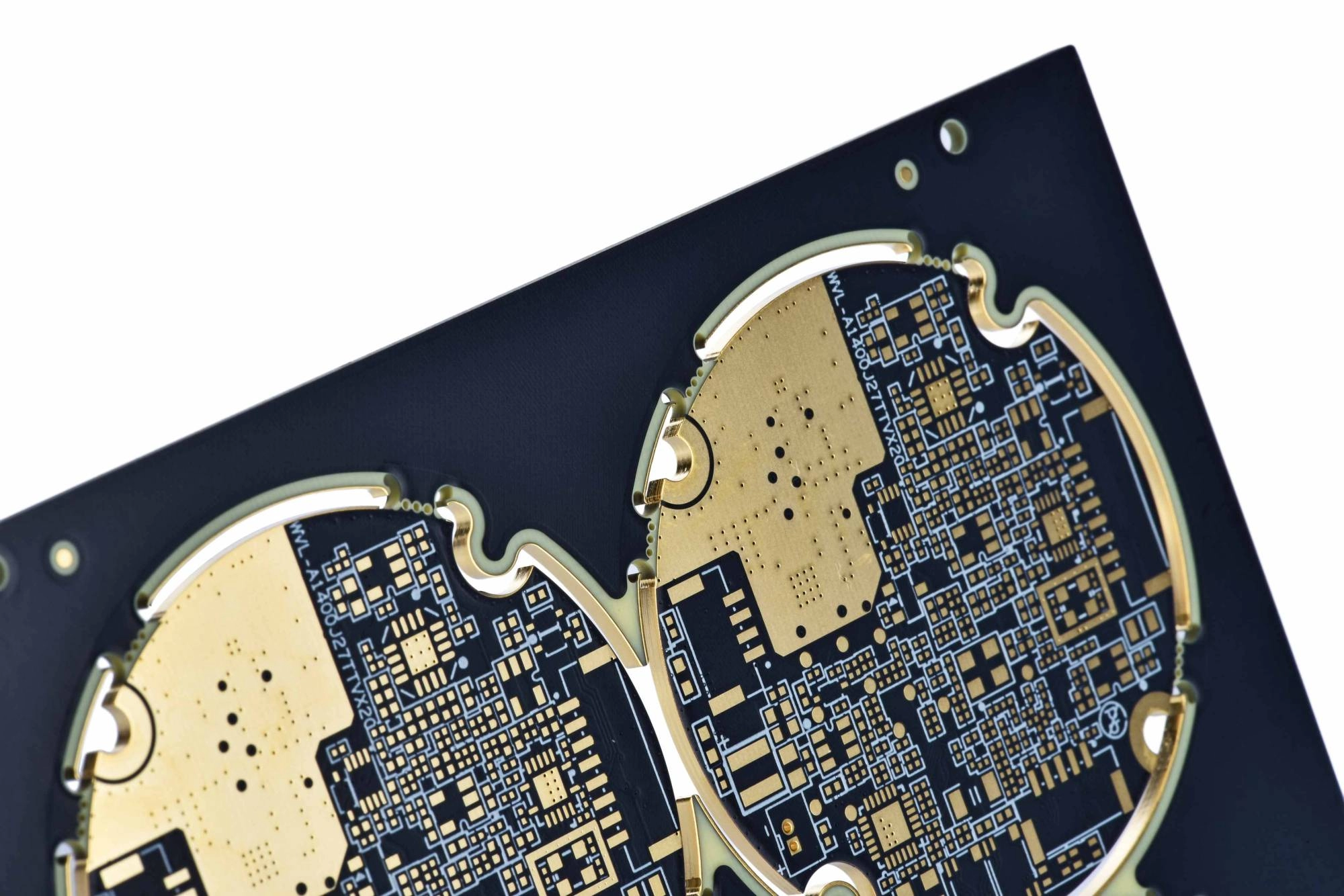
HDI PCB example from KnownPCB's HDI PCB page.
Also distinguish the electrical connection from the manufacturing access needed to form it. The artwork may show a pad on L2 and a connection from L1, but the process still has to expose the target, prepare the opening and form its copper connection. If another layer is added first, the access and hole depth change.
A layer-pair list should identify the hole technology and any filling requirement as well as the endpoints. Mechanical drilling and laser drilling have different access and geometry constraints. A filled structure used beneath another microvia requires additional processing decisions; it cannot be represented adequately by a single hole symbol that omits the intermediate layers.
Altium's comparison of sequential lamination and sub-lamination describes how via access and the order of bonding, drilling and plating differ between construction methods. Use those distinctions when discussing the route with the fabricator, rather than assuming that every blind-via design follows the same process.
An inner connection that will be covered by later material must be completed at an earlier stage. Identify the inner structure in which that hole can be drilled and plated. At this point it may pass through that smaller structure; after additional layers are bonded around it, the same connection is buried within the finished board.
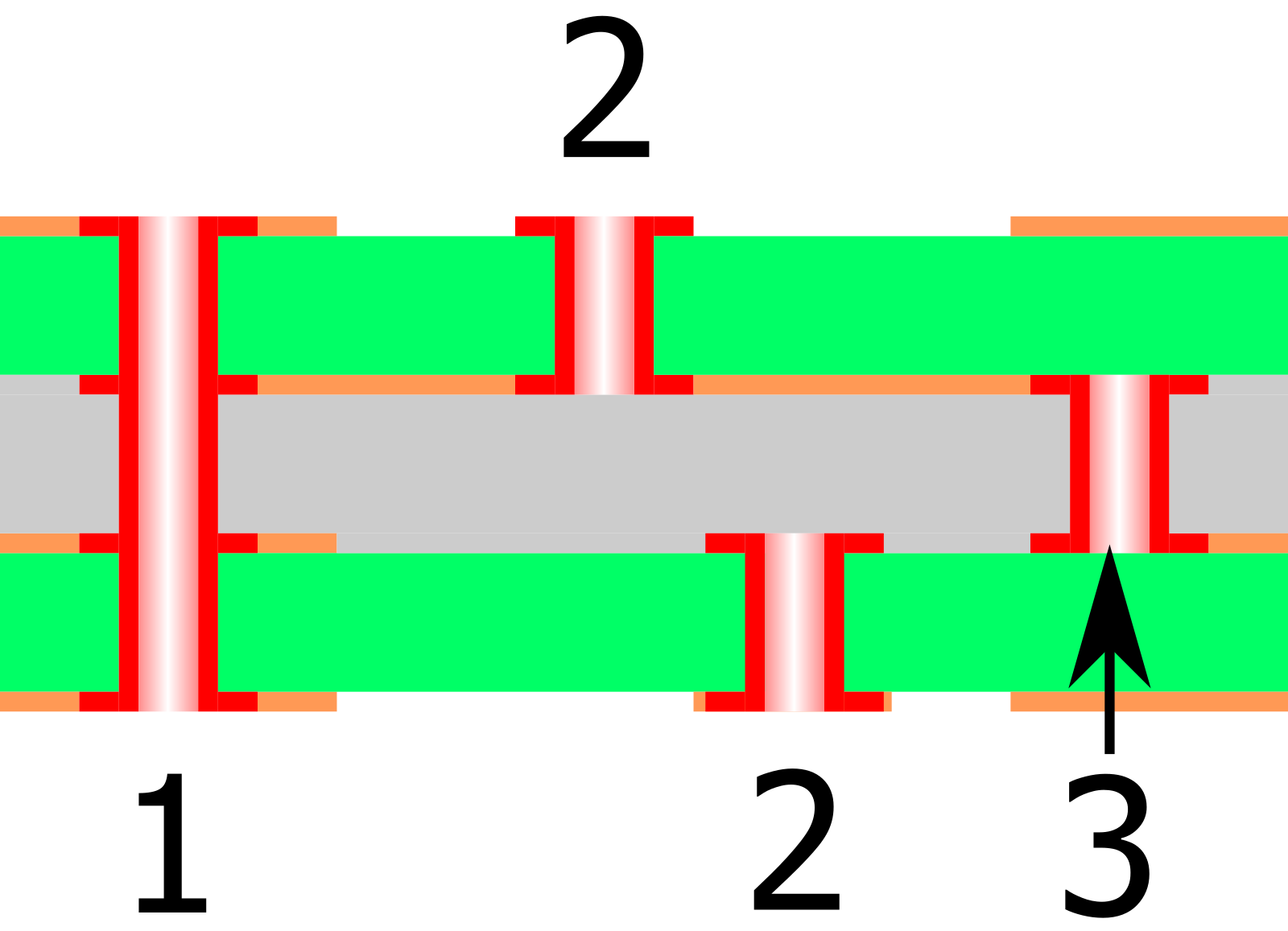
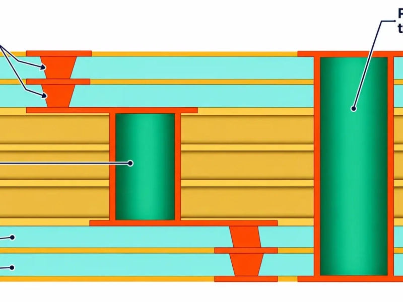
PCB via types diagram by M. Adler, shared under CC BY 3.0; original file.
This is why the word "buried" describes the hole's position in the completed board rather than a drilling operation through an already finished outer surface. The process plan has to establish the inner stack before it can establish the buried connection. It must then preserve the connection through the later bonding and processing steps.
Keep a sub-stack's layer names traceable to the final names. An intermediate fabrication file may call its two outside surfaces top and bottom, while the final drawing calls them L2 and L5. Record that mapping explicitly. A hole program can otherwise appear to match a sub-stack while its endpoints disagree with the released board definition.
Do not merge mechanically drilled buried connections and laser microvias into one aspect-ratio calculation. Their depths, entry conditions and manufacturing stages differ. The existing microvia aspect-ratio article covers the geometry question separately; the task here is to establish access and sequence.
Consider a teaching example with six final copper layers. The design includes a buried connection across an inner L2-to-L5 structure, blind connections from L1 to L2 and from L6 to L5, and a final through hole. The table follows those connections through possible processing stages. It specifies a logical dependency, not the material recipe or press program for a production order.
| Stage | Accessible structure | Connection to complete | Information to retain |
|---|---|---|---|
| Prepare the inner structure | Final layers L2 through L5 are identified in a sub-stack | Inner circuitry and the required buried-hole span | Final-to-intermediate layer mapping and inner drill data |
| Complete the inner connection | The hole is accessible through that sub-stack | Hole preparation, copper connection and any specified filling | Inspection and processing state before covering the structure |
| Add the outer build-up | New outer material is bonded around the prepared inner structure | Access from L1 to L2 and from L6 to L5 | Build-up dielectric, target pads and corresponding hole files |
| Complete the full-board holes | The approved final layer set is present | Specified through-hole connections | Final hole table and finished-board requirements |
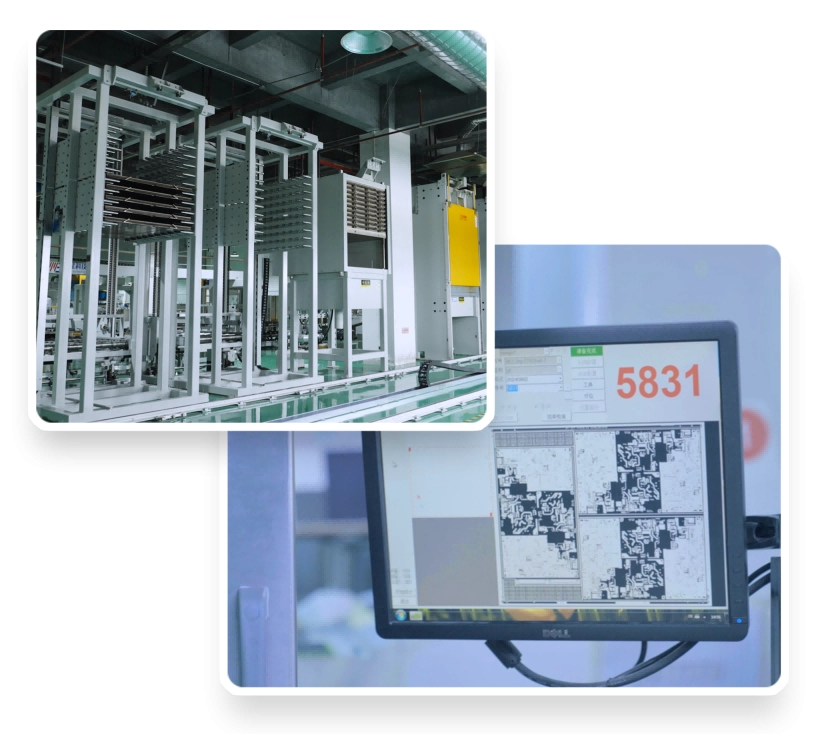
Production equipment shown on KnownPCB's multilayer PCB page.
The fabricator may divide the inner structure into additional sub-laminations or select a different compatible route. The engineering question is whether the proposed sequence preserves every required connection and permits the necessary hole processing. Approve that route before releasing a layout built around assumptions about which holes can coexist.
Now add a second outer build-up layer on each side. A connection between two earlier build-up layers must be formed before the next dielectric covers its entry surface. If the later microvia is placed directly over an earlier one, the underlying feature must have the required filled and prepared condition before that later connection can be fabricated.
This adds a dependency to the schedule. It does not mean that the text "2+N+2" alone specifies the total number of press operations. The central structure can have its own earlier processing, and the actual route also depends on the hole spans and materials. Ask for the sequence of intermediate structures, not just a count of finished layers or a marketing description of HDI order.
Altium's layer-stack construction overview distinguishes build-up structures from constructions assembled using sub-laminations. That distinction helps explain why a final layer diagram and a press-count label cannot replace the process route.
Prepare one controlled layer map, then associate the individual hole data with the corresponding stage. State the start and end layers using the released names, identify plated and nonplated features, and separate mechanical hole data from laser-hole data where the manufacturing handoff requires it. The file set should let a reviewer locate each hole structure without interpreting an unexplained filename.
Include filling, capping and local planarization requirements where they affect a subsequent connection or a surface pad. Those requirements influence what must be completed before the next layer is added. Keep the detailed acceptance conditions in the fabrication drawing or agreed specification, rather than relying on an image of a generic via type.
A change to a via span can change more than the drill data. Moving an endpoint may require a different inner grouping, an additional build-up stage or a revised copper-processing sequence. Recheck the material and finished-copper assumptions for the affected layers when approving that change.
Keep electrical acceptance separate from the visual appearance of a via illustration. The illustration explains the connection type. The fabrication record must identify the actual hole, layer pair, process stage and required inspection for the released construction. A photograph of equipment cannot establish that an intermediate buried connection has passed its acceptance checks.
Review the layer-pair map with the proposed intermediate structures. Confirm that every target is accessible at the stage where its hole is formed, that earlier connections are in the required condition before burial, and that the final hole file agrees with the complete stack. Resolve an incompatible span before fine routing makes the change expensive.
The existing HDI stackup manufacturability article provides the broader construction context. Keep the sequential-lamination review focused on the order of operations and file mapping, rather than repeating the general reasons to select an HDI stackup.
Submit the proposed stackup, hole layer pairs, filling requirements and controlled fabrication revision for review against KnownPCB's HDI manufacturing capabilities. A useful response should address the actual construction and any changes needed to make its sequence manufacturable. Confirm the scope and acceptance requirements with the engineering team before releasing the production files.
October/09/2026ENIG Black Pad: Inspection and Lot Traceability

April/24/2026Aluminum vs Copper vs Stainless Steel MCPCBs: Thermal Performance, Cost and Applications
March/20/2026Automotive Multi Camera System Demands and Challenges in PCB Process
March/10/2026How 0.2–1.2 mil Solder Mask Thickness Affects 100 Ω Differential Impedance and Insertion Loss
November/05/2026PCB Manufacturing Process: DFM to Bare-Board Test