
The PCB manufacturing process turns released design data into a bare board through a sequence of linked stages. File review defines the layer build and tooling data. Patterning forms the copper circuits, lamination joins the layers, drilling and plating create interconnections, and finishing protects the exposed board. The final electrical test checks the fabricated net connections against the released design data.
The exact route depends on the layer construction, hole structure, material and finish. The process map below describes a common multilayer bare-board flow. It names the input, the main action and a useful release check at each stage. It does not cover component assembly.
On this page
| Stage | Main input and action | Check before handoff |
|---|---|---|
| DFM and material review | Released design files, construction and acceptance notes are reviewed for tooling. | Resolve file, revision, layer and drill mismatches. |
| Inner-layer pattern | Copper foil receives the layer image and unwanted copper is etched away. | Compare each finished pattern with its source layer data. |
| Lamination | Core, prepreg and copper are arranged and bonded as the approved stack. | Confirm order, alignment and finished construction. |
| Drilling and plating | Holes are drilled, prepared and plated to connect the specified layers. | Check hole data, via span and plating-related queries. |
| Outer pattern and finishing | Outer copper is formed, then mask, finish, legend and profile are applied. | Reconcile exposed features and outline with released files. |
| Bare-board test | The fabricated connections are tested against a defined netlist. | Use the approved revision and record unresolved failures. |
Before tooling is prepared, the fabricator needs a controlled definition of the board. That normally means a current revision of the copper images, drill data, outline, stackup and fabrication notes. The files should describe the same board. A mismatched layer label or an unexplained difference between the drill file and the drawing needs a question before the job moves forward.
The front-end review checks whether the data can be translated into a manufacturing route. The layer count, material build, copper requirements, hole types, surface finish and outline all affect the work that follows. The fabricator prepares the image, drill and other tooling information from the released data. Altium's fabrication overview describes this front-end engineering step and the tooling it prepares.
Keep the review tied to a named revision. If a netlist, layer name, board outline or acceptance note changes, identify the affected files and approve the replacement set. Do not let the process traveler or email subject become the only record of which design is being built.
The design team should also know which questions are still open. A fabricator may ask for a missing stackup field, a drill interpretation or permission to adjust a geometry. Record the answer against the same revision. This keeps a design decision from becoming an undocumented process assumption.
For a conventional multilayer board, inner-layer copper starts on laminate with copper foil. A light-sensitive coating receives the layer artwork. Exposure and development leave the pattern that will remain; etching removes unwanted copper. The resulting layers are inspected against their design data before the stack is assembled. The inspection looks for opens, shorts, missing features or differences that should be resolved before lamination.
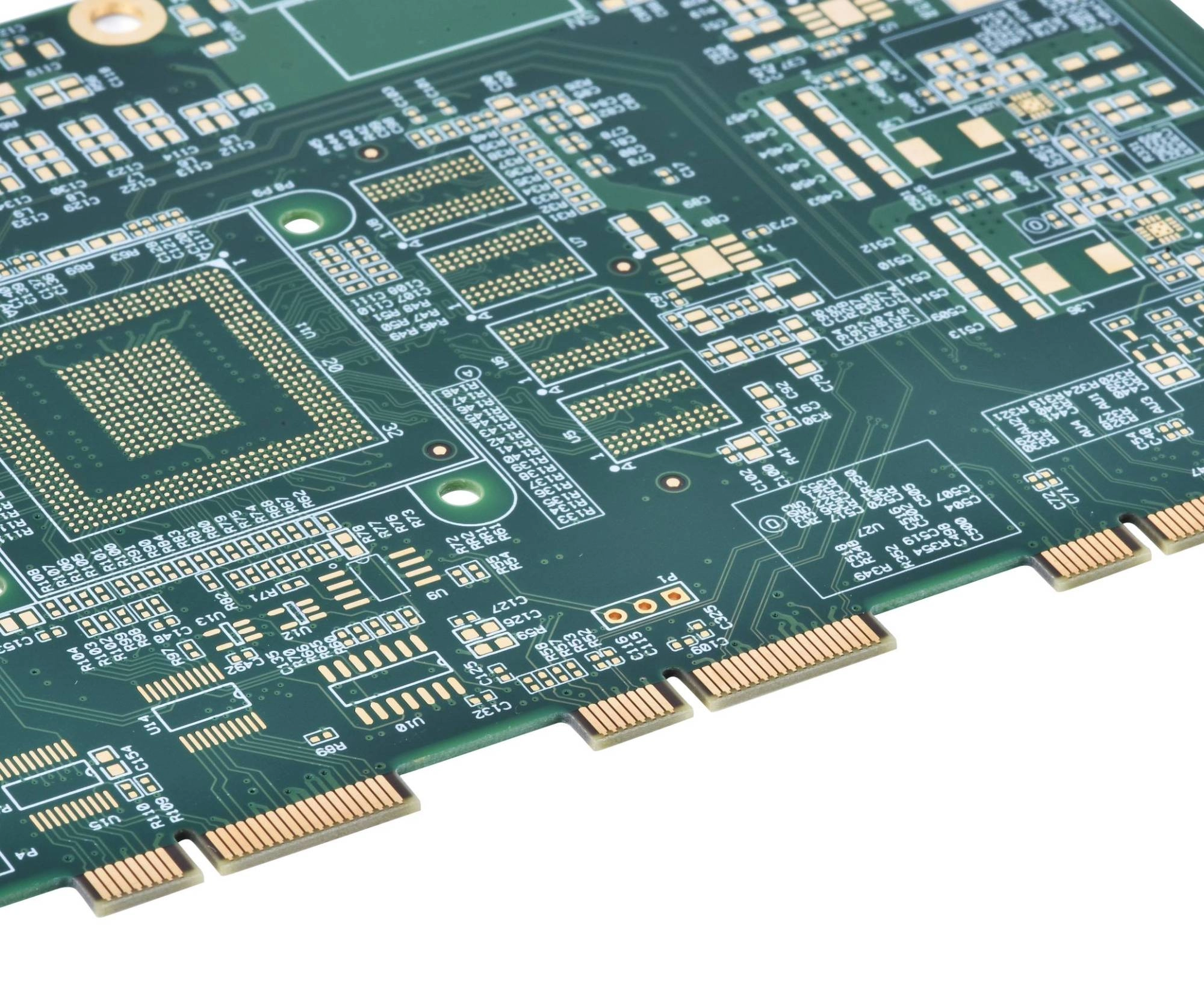
Multilayer PCB panel photo from KnownPCB's multilayer PCB page.
The inner surfaces also need preparation so the layers can bond during lamination. The exact chemistry and control method depend on the material and process route. This is a bond-surface step before stack assembly; it is separate from removing drill smear from hole walls after drilling.
Before releasing the layer pair to the next stage, check that the artwork revision, layer identity and inspection result agree. A panel can carry several board images and process features around the product outline. Those tooling features support alignment and production handling, but they do not change the need to check the design data that defines the finished board.
Inner-layer inspection verifies the patterned copper, but it does not prove that the finished board is electrically complete. Connections between separate layers do not exist until the board has been laminated, drilled and plated. Keep each check associated with the stage where it can answer the question.
In a typical multilayer build, copper-clad cores and partially cured prepreg are arranged in the specified order. The press applies heat and pressure so the resin bonds the layers and fills the spaces between copper features. The finished stack is then drilled according to the released hole data. Layer count, via span and any sequential build-up features can change how many layup, lamination and drilling operations are needed.
Drilling exposes the copper layers that a plated hole must connect. The hole wall can carry resin smear, so the desmear step prepares it before metallization. A thin electroless copper deposit acts as a conductive seed. In a pattern-plating route, later imaging controls where electrolytic copper is built on the surface and in the holes. The methods and order depend on the board construction. The drawing should identify the required hole type, connected layers and finished condition instead of assuming that every hole is the same. See the separate desmear process guide for the hole-preparation details.
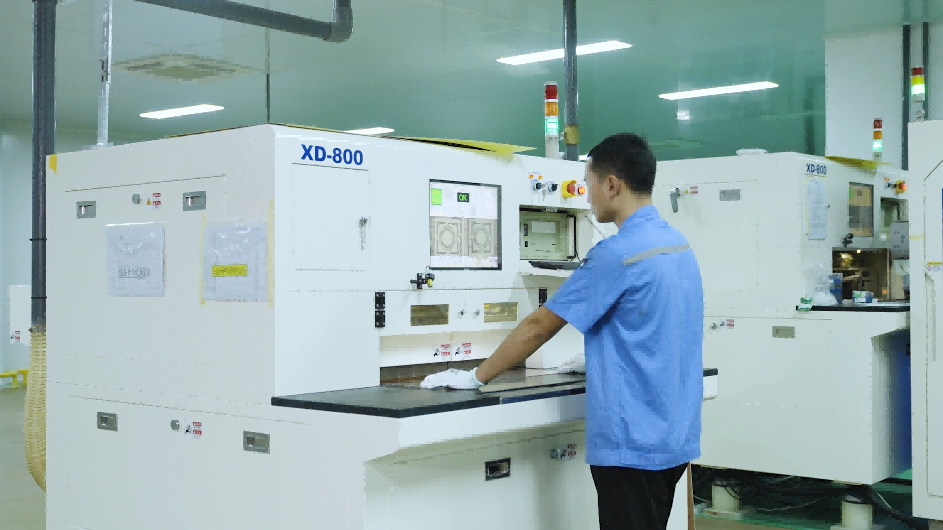
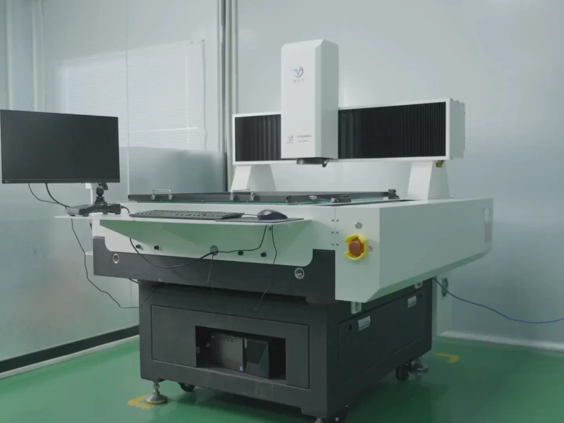
X-ray drill-targeting equipment shown on KnownPCB's company profile page.
At this overview level, the checks are simple: compare the stackup to the released layer list, confirm each plated hole has a defined span, and review the drill and plating data against the design. For inspection methods and defects, link to the specific hole-wall quality guide and plating-voids article. Those pages cover their own technical questions in detail.
Some constructions require additional build-up cycles or a different drill sequence. This map does not prescribe those routes. The process notes and released stackup must identify any special sequence before tooling is prepared.
In a common pattern-plating route, the outer-layer image exposes selected conductor features after the hole walls have received their thin seed deposit. Electrolytic copper then builds the required surface conductors and plated-hole barrels. The resist is removed and unwanted copper is etched away. This later pattern-plating step is distinct from the initial seed deposit; other production routes may arrange operations differently. The finished copper must match the approved layer artwork and construction.
Solder mask covers areas that are not intended to remain exposed. The specified surface finish protects the exposed copper pads until assembly. Legend printing, routing, slots, edge features and depanelization complete the board profile. These are separate data sets and notes, so the fabricator needs consistent revisions for outline, mask, finish and any non-plated mechanical holes.
A final visual or dimensional check can catch a mismatch between the outline, holes and finished panel. This does not replace the designer's acceptance requirements. If a dimension or finish callout conflicts with a file, pause for a written resolution rather than choosing one source silently.
Surface finish, mask openings and legend are separate layers or notes in the release package. They should match the intended pads and manufacturing route. A finish name alone does not specify the full acceptance criteria, so any inspection method or certificate request belongs in the controlled requirements rather than being assumed from the process map.
Electrical test checks whether the finished copper connections agree with the intended circuit data. A bare-board test can compare measured connections against the design netlist to find opens or unintended shorts. A fixture with fixed contacts or a flying-probe system may be used, depending on the board, quantity and production setup. Those methods are not interchangeable with every other electrical or reliability test.
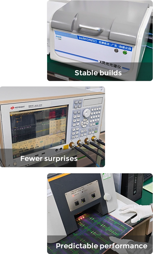
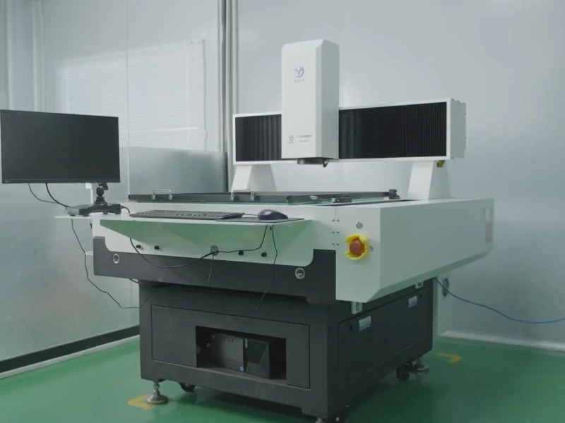
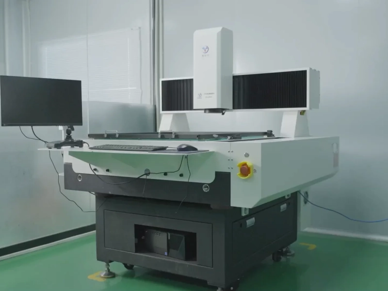
PCB quality-control equipment from KnownPCB's quality-control page.
The test program must use the same approved revision as the board artwork. If the netlist, test points or allowed connections changed after the test data was prepared, the tester may check the wrong design. Define what is tested, which revision is used and how a failure is recorded before accepting results. Altium's bare-board process overview describes netlist-based opens-and-shorts testing at the end of fabrication, before the separate assembly section.
A continuity test checks the board's intended electrical connections. It does not by itself prove RF performance, assembly function, insulation withstand or compliance with every product requirement. State the test purpose and acceptance basis separately. If the board requires an additional electrical or reliability test, identify the test object and responsible party before release.
A practical release review can follow the board from start to finish: confirm the file set and material build, verify inner-layer artwork, check the plated-hole construction, reconcile the final outline and surface treatment, and match the electrical test to the released netlist. If a stage raises a detailed question, use the relevant process guide instead of repeating the whole topic in this overview. For KnownPCB's multilayer service, see the multilayer PCB manufacturing page. Use the contact page to discuss the board files and requirements before release.
May/27/2026DFM for PCB with Large-Footprint Components
December/06/2025What Are The HDI Board Risks for Radar Modules
October/21/2026PCB TDR Impedance Test: Read the Lot Report
October/22/2026Double Sided Metal Core PCB: Layers and Hole Isolation
October/08/2026Single-Sided vs. Double-Sided PCB: Routing and Cost