
Single-sided and double-sided PCBs differ first in how many copper faces carry circuit patterns. A single-sided board places its conductive pattern on one face of the laminate. A double-sided board can route on both outer faces and connect them through plated holes. Compare crossover needs, return paths, board area, and quote assumptions. One copper face does not guarantee a lower price at every order quantity. This article covers bare-board construction and fabrication cost. The side used for components does not determine copper-layer count.
Table of contents
A single-sided PCB has a circuit pattern on only one copper face. The other face may carry legend or components, but that does not add another conductive layer. A double-sided board can route on both outer copper layers. If a connection must move from one face to the other, the design uses a plated hole. A standard mounting hole may be nonconductive, so the fabrication drawing should distinguish plated holes, non-plated holes, and mechanical locating holes.
That distinction affects Gerber data, drill files, and quoting. You cannot reliably determine layer count from a top-side photo, and components mounted on both sides do not define copper-layer count. State the copper-layer count, copper thickness, and hole types in the stackup and fabrication notes. To check KnownPCB's current single-sided product scope, see its single-sided PCB page.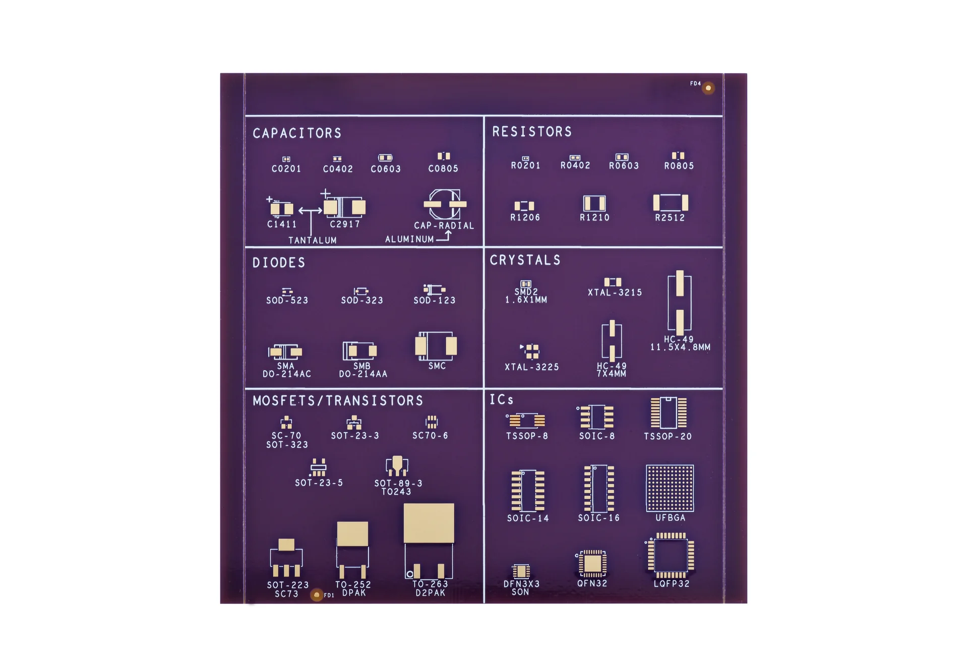
KnownPCB 2-layer S1000H ENIG PCB product photo. The image shows the finished surface, not the internal copper layers.
On a single-sided board, two traces on the same copper layer cannot cross. The designer must change component placement or routing order, or add a jumper wire or zero-ohm resistor. Each jumper affects the drawing, pad location, and assembly notes. Too many jumpers can make the layout harder to review and revise.
A double-sided board can move some nets to the other face and use plated holes to change layers. The KiCad PCB Editor documentation explains how to route on different copper layers and switch layers with vias. Hole diameter, annular ring, and trace clearance still need to match the fabricator's confirmed rules. A second routing face adds routing options; it does not automatically shrink the board outline or remove every conflict.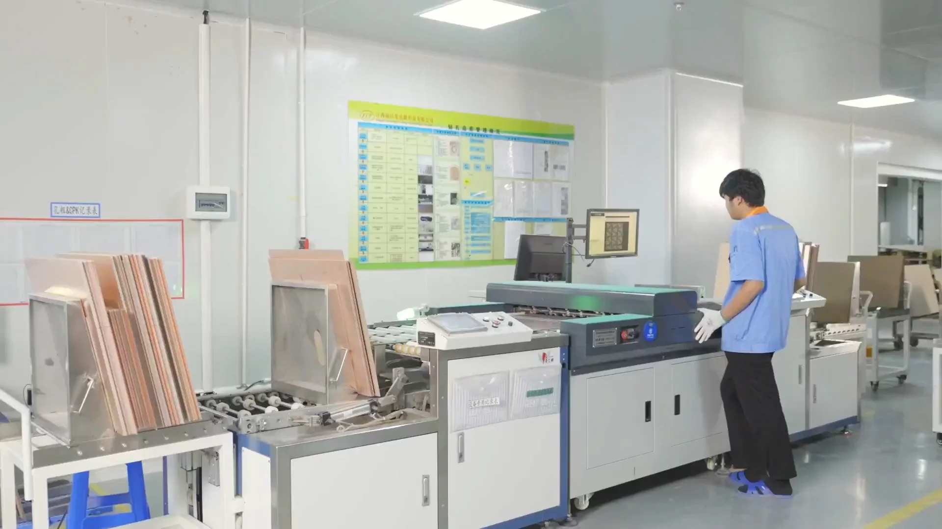
PCB drilling inspection station. The equipment photo does not show whether a particular hole is electrically connected.
Single-sided and double-sided boards use different fabrication routes. A double-sided board needs circuit patterns on both faces and conductive connections through specified holes. A single-sided board usually does not need an electrical connection between its two faces. These process differences can affect cost, but the quote also depends on laminate, copper thickness, hole count, minimum trace width and spacing, surface finish, panelization, and order quantity. Do not apply a percentage from another order to your own design.
For a useful comparison, ask both fabricators to quote against the same files and requirements: outline, material, finished thickness, copper thickness, finish, solder-mask color, hole definitions, quantity, and delivery date. Confirm whether the single-sided construction is part of the shop's standard route and whether jumpers or special board edges add charges. At low quantities, setup, panel utilization, and minimum-order fees can outweigh the difference between one and two copper faces.
Keep engineering charges separate from fabrication charges. A change in copper-layer count can change the Gerber review, drill files, and process route. Design effort and electrical-test requirements can also affect the quote. Compare the total order and expected repeat quantity instead of carrying one small-batch price into a production forecast.
Board current capacity, signal integrity, and noise cannot be reduced to copper-layer count. Current capacity depends on copper thickness, trace width and length, and heat removal. Return paths depend on the relationship between signal traces and reference copper. A second copper face does not automatically provide a continuous reference plane. If the design is near an electrical limit, confirm the stackup and design rules, then review the finished routing with the electrical designer.
When two options use different board outlines, include panel utilization in the comparison. A larger single-sided design may fit fewer units on a production panel because traces need more room to avoid crossings. A more complex double-sided route may use panel area more efficiently. Quote each finished outline rather than treating copper-layer count as the only changed variable. Ask the fabricator to separate first-run charges from repeat-order charges.
Lead time also depends on the shop's actual production route. Removing a plating step does not guarantee faster delivery if the material, solder-mask color, or surface finish requires a separate production slot. Ask about the planned start date, inspection scope, and delivery date for this order.
A single-sided board can fit a circuit with simple connectivity, enough board area, and current and signal paths that can be arranged on one copper face. It can also suit a mature design that needs to keep its existing interfaces and mounting dimensions. Do not choose by component count alone. One component with many pins can create multiple crossovers; a small circuit can still be difficult to route on one face when connector locations are fixed.
Place the critical interfaces first, then try routing on one face and record the nets that cannot connect directly. If placement changes still leave many jumpers, or the ground, power, and sensitive signal paths compete for the same narrow area, quote a double-sided option as well. Check current, frequency, and return-path requirements. A connected net is not by itself proof that the electrical layout is acceptable.
A double-sided board is often easier to route when the netlist has many crossings, connector positions are fixed by the enclosure, or one-layer routes would become long. The second face can also carry a ground grid or copper region, but the designer must check whether the copper remains connected and whether return current must detour. TI's Practical PCB Design Rules explains that a slot in a reference plane can divert return current and increase loop area. Two copper faces do not automatically create a complete ground plane.
If the design needs a stable reference plane, controlled impedance, low crosstalk, or dense power distribution, choosing between one and two copper faces may not be enough. Evaluate additional layers, a revised stackup, or new trace locations. Layer count determines the available structure; it does not guarantee electrical performance.
Revision frequency is another selection factor. Adding an interface to a single-sided board may force traces across existing nets, requiring component moves or more jumpers. A second copper face can relieve some crossings, but each via still occupies a pad and surrounding clearance. Reserve interfaces, mounting holes, and critical power paths, then estimate how much usable routing space the second face adds.
Run manufacturability checks and electrical checks separately. Design-rule checking can find spacing, connectivity, and hole-definition errors, but it cannot decide whether a return path is sound or shared ground impedance will disturb a sensitive signal. If the design relies on a continuous copper region as a reference, inspect whether pads, traces, or mounting holes cut that region into narrow necks or isolated islands.
Before release, check that copper-layer count, Gerber files, drill files, board outline, hole attributes, finished thickness, copper thickness, surface finish, and special notes agree. For a double-sided board, identify which holes need electrical plating. For a single-sided board, make sure every net uses the allowed copper face and each jumper has a defined pad and installation note.
For prototype builds with several designs or revisions, ask KnownPCB's high-mix, low-volume prototype service to quote the single-sided and double-sided constructions as separate options against the same data. Check the inspection and lot-record scope on KnownPCB's quality management page. If the drawing boundary or quote assumptions need clarification, contact KnownPCB's engineering team.
No. A single-sided board avoids electrical connections between copper faces, but the quote also depends on material, outline, quantity, surface finish, and production schedule. Compare the same order conditions rather than applying another buyer's price ratio.
More routing space can reduce detours and may allow a smaller outline, but footprints, connectors, heat removal, and mounting holes constrain the layout. Compare the board outlines after routing and mechanical review.
No. Copper-layer count describes the conductive faces used by the circuit. Components can be mounted on only one side. This article compares bare boards; component placement sides and assembly operations should be quoted separately.
March/04/2026RFPCB Optimization for Ultrasound Probe Medical Devices
September/24/2026PCB Hole Wall Roughness: Causes, Inspection and Plating Risks
March/10/2026How 0.2–1.2 mil Solder Mask Thickness Affects 100 Ω Differential Impedance and Insertion Loss
June/24/2026High-current Heavy Copper PCB

September/28/2026PCB Annular Ring Breakout: Causes, Layer Inspection, and DFM Checks
