
In PCB production, a plated through-hole can pass the finished-hole diameter check and still cause concern at final inspection. Under magnification, the hole may sit close to one edge of its pad, leaving almost no copper on that side. A correct diameter tells us the hole is the right size. It does not tell us whether the hole lines up with the pad on every copper layer. Once the hole crosses a pad edge, we need to identify the affected layer and hole, then check the copper connection to the plated hole wall.
The outer and inner layers of the same board may show different results. We compare the measured location with the product class and the customer's drawing before deciding what the finding means. A breakout alone does not justify scrapping an entire panel, and a passing hole-diameter result does not justify releasing it.
Table of Contents
The pad diameter in a design file is a target before fabrication. On the finished board, we need the actual hole position and pad boundary. We also need to know whether the finding is on an outer or inner layer. A report saying only that the designed pad was large enough cannot replace a measurement, and an unlabeled sketch cannot show which layer was inspected.
KnownPCB has already covered weak annular rings as one of several PCB DFM mistakes. Here we look only at hole-to-pad registration, the copper left around a drilled hole, and what the inspection result means for that board.
Consider a hypothetical outer-layer pad with a diameter of 0.60 mm and a finished hole of 0.30 mm. If the hole and pad are concentric, the nominal copper ring is 0.15 mm on each side. Move the hole toward one edge and the ring narrows on that side while it widens on the other. The two sides are no longer symmetrical. This example explains the geometry; it is not a KnownPCB capability claim or an IPC acceptance limit.
The same calculation cannot simply be transferred to an inner layer. Outer-layer inspection looks at the finished plated hole edge, while inner-layer assessment uses the drilled hole relative to the inner pad. Drill diameter and finished-hole diameter are different values. Engineering should check each layer against the board thickness, hole structure, and agreed manufacturing allowance.
For a multilayer PCB, the inner-layer patterns are formed first. The layers are then stacked and laminated before the through-holes are drilled. Each patterned layer has its own registration target, and the panel can change size during lamination. A drilling machine may hit its target while one inner-layer pad has already moved relative to the planned hole center. In that case, adjusting the drill alone will not correct the earlier layer-to-layer displacement.
When investigating an offset, our engineers compare inner-layer registration records, lamination compensation, and drill-targeting records. An outer layer with sufficient copper around a hole does not prove that every inner layer has the same margin. We check connected inner-layer pads individually because a narrow or broken ring can affect their connection to the plated hole wall.

Drill targets are checked before production drilling. This equipment photo does not show an annular ring breakout defect.
During drilling, the question is whether the actual hole center falls where the program expected. A worn drill, unstable panel clamping, movement in the drilling stack, or a mismatch between the drill target and the copper pattern can shift a hole toward the pad edge. Yet an off-center hole does not prove that the drilling settings are at fault. The offset may have started during inner-layer imaging or lamination.
We compare hole positions across the panel. Is the problem concentrated in one corner? Does the offset grow in one direction, or does it occur at only a few holes? Target measurements, drilling records, and other boards from the lot help answer those questions. Repeated results give the factory a better basis for deciding which process to adjust than a single photograph does.
If the same panel also shows burrs, rough hole walls, or diameter drift, review the broader PCB drilling quality and hole performance records. Breakout assessment still needs the pad geometry and layer registration data for the affected hole.
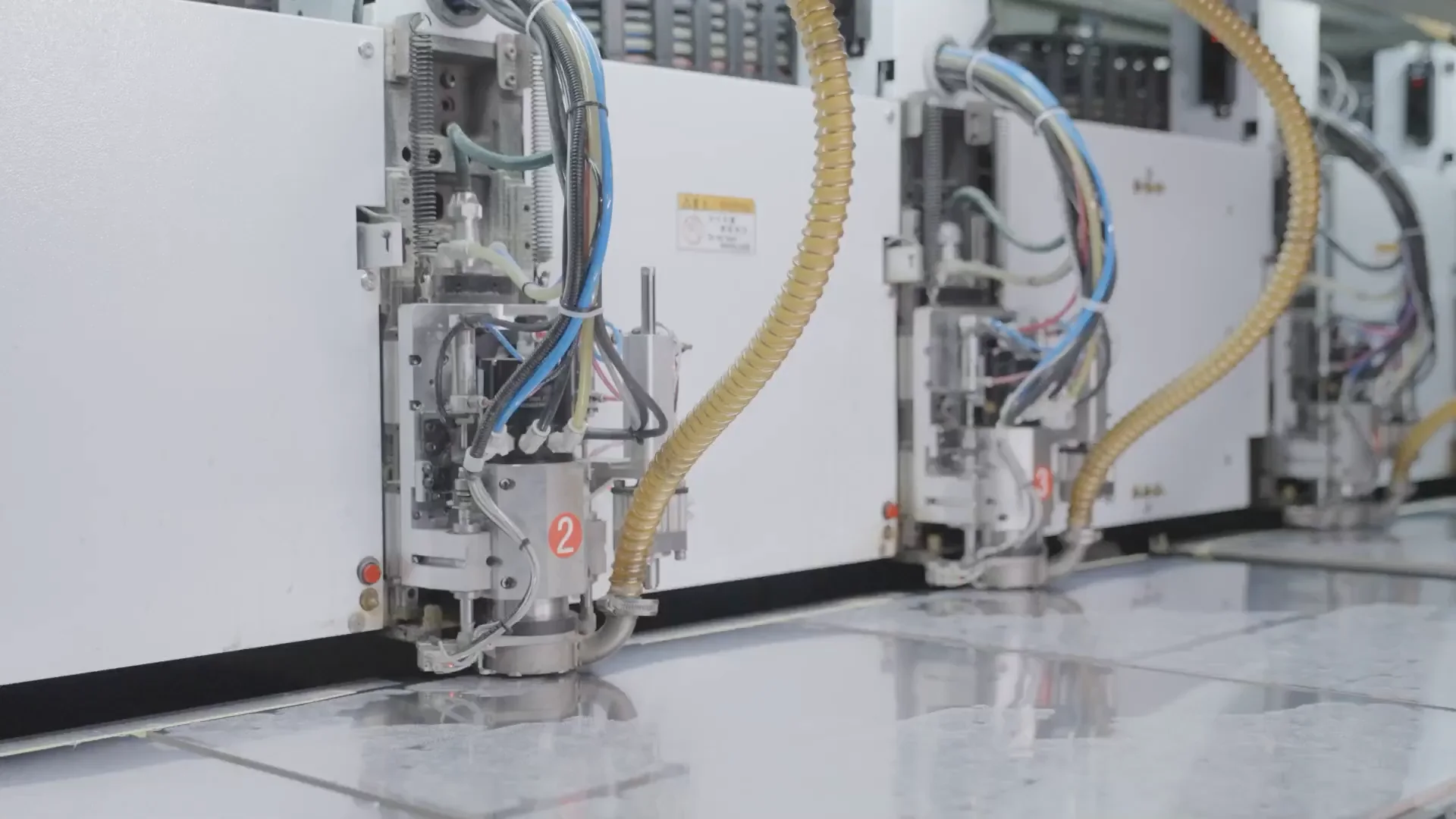
Drilling is one part of hole-to-pad registration. Pad layout and layer movement also need to be checked.
An inspection report must let another engineer find the same hole. Record the board or panel number, hole number or coordinates, affected copper layer, and whether the pad connects to a trace or copper plane. Add the finished-hole requirement from the drawing, the measured position, and the sample location. A note that says only "the annular ring is small" gives the next person a conclusion without enough information to reproduce the check.
For an outer layer, record the narrowest remaining copper ring and include the corresponding image. For an inner layer, state the section direction and measurement method. If several holes or panels show an offset in the same direction, show where those findings occurred. An isolated hole and a repeated registration shift require different investigations.
A cross-section shows the sampled hole wall, copper layers, and annular ring visible in the plane that was cut. It covers one location and one section direction. If the largest offset lies elsewhere around the hole, a section that looks acceptable may still miss the breakout.
We compare the section with plan-view position data, drill targets, and other samples. If a real breakout microsection is used as an illustration, it should identify the hole, layer, cutting direction, and magnification. Photos of drilling or inspection equipment explain the process but are not evidence of the defect itself.
An IPC technical paper on breakout angle explains why internal-layer registration cannot always be judged from a conventional vertical microsection alone. Record the inspection method before interpreting a breakout angle or comparing two reports.

Drilling inspection results should be considered alongside layer-registration and cross-section records.
Whether a breakout can be accepted depends on the specified product class. IPC requirements differ by class, and the inspection of outer and inner layers is not identical. For a finished order, we first confirm the standard revision and class named by the customer. Drawing notes and purchase requirements may set tighter conditions.
If the order does not state a revision or class, the inspection report can still describe the breakout location, extent, and measurement method. It should not declare the board "IPC compliant" or "IPC noncompliant" without an agreed criterion. Any pass or fail decision should cite the requirement that applies to that order and be checked by engineering or quality staff.
Altium's IPC-6012 annular-ring explanation separates external-layer and internal-layer measurement. Use it to understand the geometry, then apply the revision and acceptance class named in the customer's order.
At the design stage, the pad needs enough room for drilling and layer registration variation. Finished-board acceptance concerns what was actually manufactured. The design allowance reduces fabrication risk; it is not itself a pass or fail measurement on a completed board.
A theoretical annular ring in the design file does not prove that the finished board meets its requirement. Likewise, a recommended design dimension should not be treated as the acceptance limit. Keep the designed pad size, agreed process allowance, finished-board measurement, and customer-specified acceptance criterion separate in the review.
A PCB layout engineer can start with the most constrained holes. Check that the finished-hole requirement, pad diameter, and NC drill data agree, then look at the copper left around that hole on each layer. If a pad also connects to a narrow trace, a hole shifted away from the trace can leave a small ring on that side. A shift toward the trace calls for a closer look at the connection. Enlarging the pad may also reduce clearance to neighboring copper, so the entire local layout needs review.
Review outer and inner layers separately. For plated holes, distinguish the drill size from the required finished diameter. If the drawing gives only a nominal hole size and omits the finished-hole requirement or tolerance, ask the customer to confirm it before production.
Dense BGA routing leaves little space to enlarge a pad while keeping clearance to nearby traces. Vias connected to an inner-layer trace need an inner-layer pad review before anyone relies on the ring visible at the board surface. Blind vias, buried vias, and via-in-pad designs may follow different drilling or lamination sequences, so the affected layers must be identified for each structure.
These holes should not all be described with one generic minimum annular-ring value. In a DFM review, mark the constrained hole locations, layer-specific pad sizes, and hole-forming method. Engineering can then decide whether the pad, hole, or local routing needs to change.
If a customer receives an annular ring breakout finding, the first request should identify the affected board, hole, and copper layer. Ask for a location-marked photograph or cross-section. Compare it with the approved Gerber or ODB++ data, NC drill file, stackup, and drawing. Without the original design data, one defect photo cannot establish whether the problem began in the layout or during fabrication. That ambiguity can delay resolution.
The inspection package should also state the standard revision and product class, measurement method, sample scope, and whether the same condition appears elsewhere in the lot. If the board fails the agreed requirement, the fabricator should explain which boards have been isolated, what was rechecked, and what corrective action is proposed. The buyer can then determine whether the issue affects one hole, one board, or a larger batch.
KnownPCB's quality-management process describes the inspection context for fabricated boards. When reporting a suspected breakout, send the marked hole location and the relevant drawing so engineering can compare the observation with the approved build data.
If your layout has a tight annular ring or an unusual plated-hole structure, send the board files for a drill-to-copper DFM review before releasing the design to production.
IPC, The Enigmatic Breakout Angle.
Altium, Meeting Standards: IPC 6012 Class 3 Via Sizes and Annular Rings.
September/24/2026PCB Hole Wall Roughness: Causes, Inspection and Plating Risks
July/10/2026Prototype PCB Assembly vs Low Volume PCB Assembly
March/20/2026Automotive Multi Camera System Demands and Challenges in PCB Process
April/09/2026Heavy Copper PCB Projects
March/04/2026RFPCB Optimization for Ultrasound Probe Medical Devices
