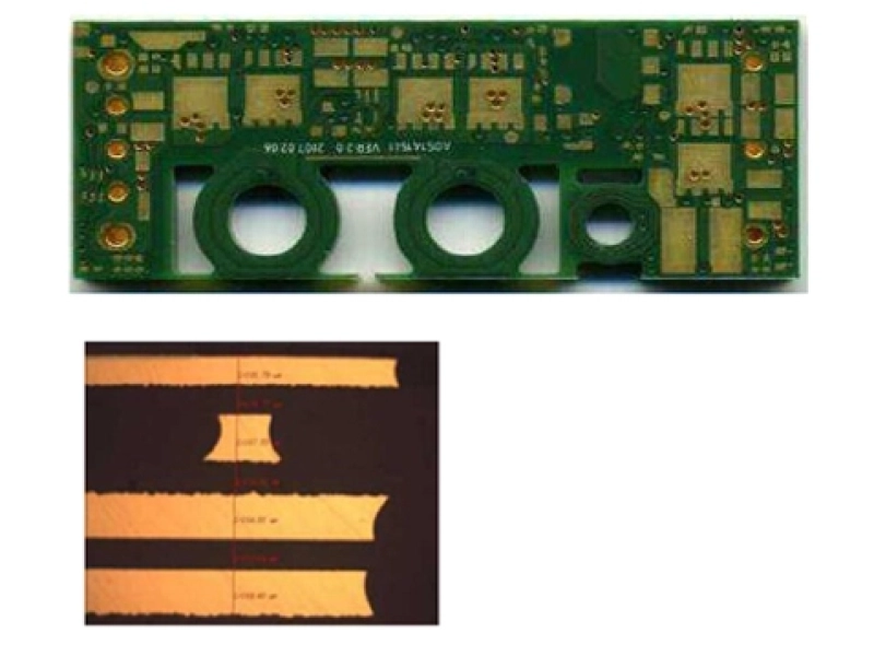
Before labeling a dark area in a plated through-hole cross-section "poor plating," locate it. A gap halfway down the barrel calls for different checks from one at an inner-layer junction or near the hole opening. PCB plating voids are areas where the required metal coverage is missing or interrupted in a bare-board plated hole. A crack that forms in previously deposited copper is a different defect.
Solder voids form during assembly. Cavities in via-fill material are another inspection issue. This article covers the copper on the walls of conductive holes in bare PCBs.
Table of contents
The copper lining of a plated through hole connects specified circuit layers. A void occurs where that metal coverage either failed to form or was lost later. Start the report with what the sample shows: the hole identifier, affected layer, position along the barrel, visible gap length in the section, and copper remaining on either side. "A void was found" gives too little information to trace its cause.
Non-plated mounting holes intentionally have no copper lining. Their exposed walls are not plating voids. Blind and buried vias can have coverage defects, but their fabrication sequences and sampling methods differ. Confirm the hole type from the approved drill data and stackup.
Several defects can look similar. A barrel crack is a fracture in deposited copper. Interface separation is a loss of adhesion between materials. A cavity in via-fill material does not necessarily mean copper is missing from the wall. Solder voids belong to the assembly process. Calling all of these "via voids" can send the investigation to the wrong production step.

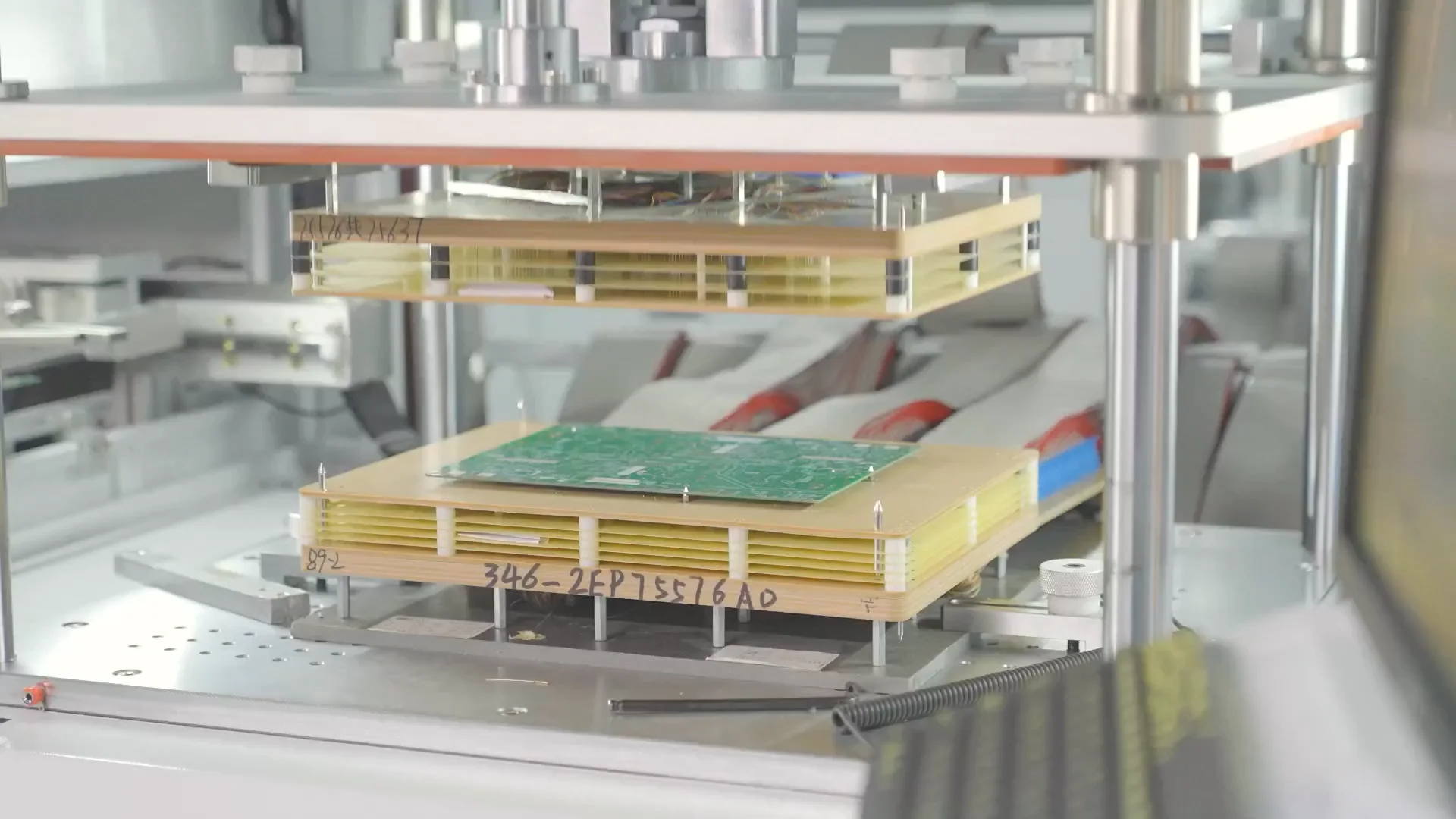
This photo shows the hole-metallization process area, not a microscopic plating void.
Follow the production sequence. Drilling forms the hole wall; cleaning and desmear prepare its surface; activation and initial copper deposition establish a conductive layer; electroplating then builds copper thickness. A void seen in the finished board may have started before the final plating step. If the initial deposit missed a small area, later copper growth may not close it into a reliable connection.
Resin smear covering an inner copper edge can prevent the deposited copper from connecting to that layer. Glass or resin debris can also obstruct local treatment. A rough wall warrants investigation, but it does not establish the cause of a particular void. KnownPCB's article on PCB hole-wall roughness explains why hole diameter and wall condition require separate checks.
When post-drill preparation shows no obvious fault, check activation and initial copper-deposition records. Incomplete solution contact, a trapped bubble, or a particle can leave a local gap in the first conductive layer. The University of Maryland CALCE note on resin smear describes one interface mechanism; other voids need a different explanation.
Solution exchange, bath condition, and current distribution affect copper growth inside a hole. Narrow, deep holes need particular attention to coverage uniformity. Thin copper in the middle of the barrel is not necessarily a void, so the section must identify what is missing and where. Copper already deposited can also be damaged during later processing or handling. Compare its appearance with the route used for that lot.
Technical author Happy Holden discusses PTH hole-void mechanisms at several stages, including failed initial coverage and later copper loss. Those possibilities need to be checked before changing electroplating bath settings.
Map the affected holes and boards before deciding which process to investigate. A dark area in one section could be an uncovered wall, a contaminated interface, or a location damaged later. Repeated defects at similar positions help narrow the search, but the pattern still needs to be compared with process records.
Review drilling, desmear, inner copper-edge preparation, and activation records first. A gap here may start with poor interface preparation or with a problem in the deposited metal. Examine the copper on both sides under magnification; the color of the dark area alone is insufficient.
Check particle control, wetting, bath entry, and the initial copper deposit. A microsection cuts through selected positions around the hole circumference. It cannot show coverage over the whole wall. Additional section directions or samples from nearby holes may be needed.
For missing metal near the opening, review surface preparation, subsequent imaging steps, and handling. If the voids cluster in one panel area, compare rack position, solution movement, the sampling map, and results from other boards in the lot. Record the distribution as an observation until the process evidence supports a cause.

Final inspection can identify boards that need further review. A factory photo does not replace a defect microsection labeled with the hole and layer.
A microsection shows the hole-wall structure, local copper coverage, and inner-layer connections in the plane that was cut. Preparing it destroys the sample, and its findings apply to that location. A normal section cannot establish that every hole in the lot is normal. When defects follow a spatial pattern, the sampling plan should cover the relevant hole types and panel areas.
Electrical testing checks continuity and isolation under the specified test conditions. It can identify an open circuit, but it cannot show the shape of a small gap in the barrel copper. A passing electrical result does not cancel a cross-section requirement in the customer's inspection plan. A failed result also cannot identify the manufacturing step that caused it. KnownPCB's quality-management page describes the broader finished-board inspection process.
Keep the original section image with the hole and layer identifiers, cut direction, copper measurements, sample-board number, and lot number. Record observations separately from suspected causes. If a second sample contradicts the first, retain both results so the next engineer can see the discrepancy.
Electrical testing verifies the tested circuit's electrical condition. A microsection shows copper structure at a sampled position inside a plated hole.
Before applying a void percentage or acceptance limit, confirm the product class, customer-specified standard revision, drawing, hole type, and inspection method for the order. The IPC-A-600 training program description includes plated-through-hole copper thickness, voids, and cracks among printed-board acceptance topics. That public page does not supply a universal limit that can replace the order's requirements.
The inspector records the finding. Engineering uses additional evidence to trace the likely process cause, and quality personnel apply the agreed acceptance criteria to decide how to handle the lot. Keep these decisions distinct in the review, even when the same team discusses them together.
Before production, supply Gerber or ODB++ data, NC drill files, the stackup, finished board thickness, and finished-hole requirements. Identify blind, buried, and filled vias separately. Include any special requirements for hole copper or test evidence so the fabricator can flag narrow, deep, or unusual holes for review. KnownPCB's high-current PCB via article discusses the design relationship between hole geometry and plating distribution.
For recurring voids, compare the defect map with drilling, hole preparation, activation, initial copper deposition, later plating, and handling records. Use the evidence to choose the process adjustment. After a clean follow-up section, retain the original defect record and inspect other positions on the panel and in the lot to check whether the correction holds.
To request a review of the hole design or inspection data, send the design files and marked defect locations through KnownPCB's contact page.
No. Plating voids concern metal coverage on the hole wall during bare-board fabrication. Solder voids occur in solder joints during assembly. The materials, process steps, and inspection evidence differ.
Electrical testing establishes whether the circuit meets the specified electrical test conditions. A microsection shows copper structure at the sampled location. Follow the order's inspection plan for the required tests.
No. Identify the spot's location and the material missing there, then review drilling, hole preparation, initial copper deposition, and later plating records. Color alone cannot establish the cause.
Happy Holden, Factors in PTH Reliability: Hole Voids.
University of Maryland CALCE, Resin Smear.
IPC, IPC-A-600 Acceptability of Printed Boards program description.