Blog & Design Guide

In PCB drilling, a via passing the hole diameter inspection does not guarantee that subsequent copper plating processes will be trouble-free. There are usually three main causes: resin smear caused by heat from high-speed drill rotation, protruding glass fiber fragments caused by dull drill bits, and pitted or uneven hole walls.
After drilling, the hole walls consist merely of non-conductive plastic and glass. The next steps include cleaning and desmear, which use chemicals to remove resin residue smeared on the walls; hole wall treatment and activation, which is similar to priming the wall with microscopic particles that help metal adhere; and finally electroless copper deposition for PTH and electroplating, which deposit a thin copper layer and then build it up until the hole can conduct electricity.
Table of Contents
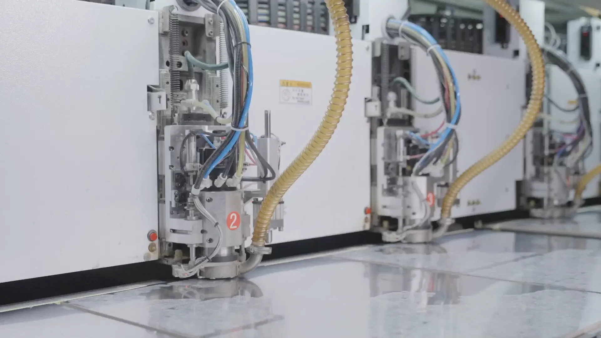
Mechanical drilling conditions affect the condition of the hole wall before the board enters later hole preparation and plating steps.
When a cross-section shows a thin or broken copper area, the investigation should begin with the sample label and production records rather than a guess about drilling parameters. First confirm the board construction, hole number, drilling records, and later copper-process records. An isolated defective hole and the same defect repeating across a panel usually do not point to the same cause.
An isolated hole issue and a defect repeated across the panel have very different causes.
If only one hole has a problem, the drill may have hit a local material flaw, or that hole may have been blocked by contamination.
If the issue appears across a panel or batch, the likely causes are incorrect drilling parameters, excessive drill wear, or a problem with the plating chemistry used for that batch.
This investigation logic is standard practice in factory quality management and failure analysis.
Hole wall roughness refers to small irregularities on the inside wall of a drilled hole. It may include resin tear-out, exposed glass fiber, and local recesses.
It is different from an entrance burr and it is different from finished-hole diameter tolerance. A hole can be within size tolerance while its wall condition still creates problems for later copper processing.
Mechanical drilling cuts resin and glass fiber at the same time. Drill condition, board construction, stack height, and the drilling program all affect the result. Laser-drilled microvias need a different review method, but the manufacturing question is the same: can the wall be prepared consistently and plated reliably for this board?
| Term or defect | Simple comparison | What actually happened | Effect on later copper deposition and plating |
|---|---|---|---|
| Resin Tear-out | Pulling a piece of cement away from the bottom of a wall and leaving a pit behind. | The drill speed or feed rate was unsuitable and tore the originally flat resin base material. | A deep recess can trap air or contamination and may cause plating voids or pinholes. |
| Glass Fiber Protrusion | Reinforcing steel in a wall was not cut cleanly and remains as a sharp broken burr. | The drill became dull and pulled the glass fiber fabric apart instead of cutting it cleanly. | Protruding glass fiber can make electroless copper coverage uneven and may contribute to microcracks visible in later cross-sections after thermal stress. |
| Micro-cavity | A small dark pit left after a fragment falls out of a wall surface. | Particle loss, contamination, or local mechanical damage. | Copper thickness may become uneven. Under high thermal expansion, local copper fracture can occur in a PTH. |
The complete process for PCB plated through holes is not described in detail here. For the full sequence, please read PCB drilling quality and hole performance. This article focuses only on hole wall roughness, inspection methods, and prevention.
Drilling is only the first step. The hole wall then goes through cleaning, desmear or other required treatment, activation, electroless copper deposition, and electroplating. When the wall is damaged or contaminated, the copper applied later may not be uniform. The issue can show up as insufficient local copper coverage, poor adhesion, or an abnormality found in a cross-section.
A 2025 study published in the Chinese Journal of Mechanical Engineering found that excessive hole wall roughness can affect later copper quality. The study also explains why many factories still use metallographic cross-sections even though the method is time-consuming and destroys the sample.
One cross-section only proves what happened at one sampled location. It does not prove that every hole on the board has the same condition.
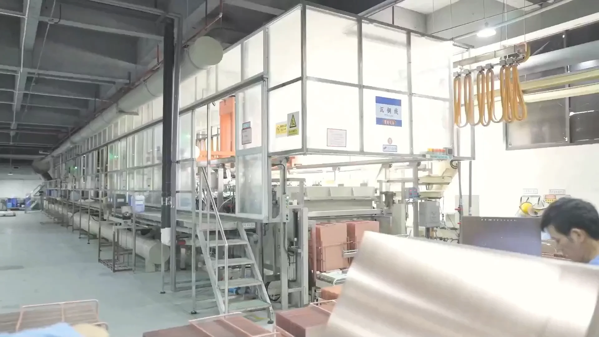
Hole preparation and initial copper deposition follow drilling. A stable drilled surface supports more consistent downstream processing.
Start with drilling records and board construction. Hole wall issues have several possible causes. If a technician changes one machine setting before reviewing the full record, the change may improve a large area while hiding the detail that caused the original defect.
Worn or dull drills may create more friction and tearing instead of a clean cut. When checking a drill, the relevant team should also review drill diameter, accumulated hit count, material type, and glass fiber structure.
A rule that works for one drilling stack may not work for another stack.
Feed rate and spindle speed affect chip removal and heat. Excessive load can damage the hole wall. Cutting too lightly can also cause drill rubbing and heat generation.
The correct setting depends on the board material actually being drilled. Settings from another board should not be copied directly into the current project.
Stack height, entry material, backup material, and panel support affect drilling stability and chip removal. Glass weave, resin type, Tg, and copper distribution also change how the drill meets the material.
If debris remains, resin smear is present, or hole wall treatment is incomplete, these issues can appear on the same wall as mechanical roughness. Their causes should be separated before action is taken.
For drilling issues, check the drill and detailed drilling records.
For cleaning or activation issues, check the subsequent hole metallization process.
Note: Do not use one universal acceptance number for hole wall roughness without context. Hole diameter, board construction, cross-section direction, product class, and the agreed inspection method all affect the result.
Cross-section inspection remains a traditional method for checking drilled and plated hole walls. Union Tool explains that the hole wall can be inspected after PCB plating and local recesses measured from a baseline. Its guidance also states that section direction changes the result. A 45-degree section along the glass fiber direction may show a higher roughness value than a 90-degree section.
Therefore, a report should not present only one roughness value. It should also state the hole type, finished-hole diameter, board material, section direction, inspection stage, and location of the maximum measured point. This is detailed work, but it is necessary.
The report should also identify whether the hole is PTH or NPTH. Burrs or diameter problems in non-plated holes are different from the wall condition and copper continuity required for plated through holes.
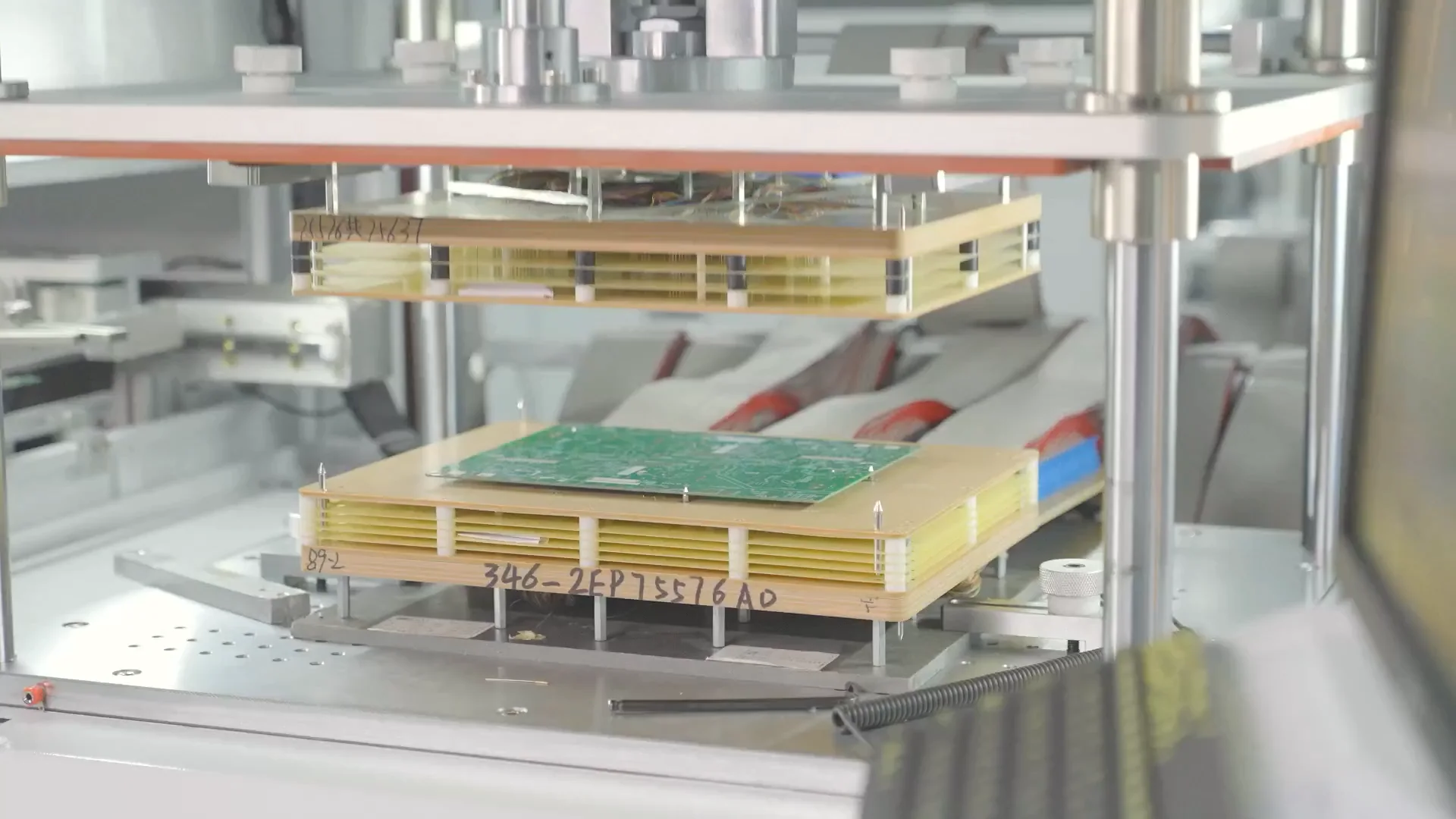
Final electrical testing is separate from cross-section inspection, but both belong to PCB hole quality control.
Engineering review should confirm board construction, finished-hole requirements, hole density, aspect ratio, special hole structures, and inspection requirements before drilling. This information helps the engineering team set the drilling plan and identify holes that need closer monitoring.
Useful process records include drill-life rules, entry and backup materials, stack height, drilling settings, chip-removal records, and inspection results. These records can accumulate into practical internal experience.
When a cross-section is abnormal, the assigned engineer should review drilling and plating records together. The investigation should follow the actual production route: drilling → hole wall treatment → initial thin copper deposition → electroplating and inspection.
For detailed factory inspection and test capability, see PCB quality-management approach.
Submit Gerber or ODB++ files, drill files, stackup, finished board thickness, copper weight, finished-hole requirements, and special test requirements. These files help the factory decide whether the hole design can be manufactured before production starts.
Blind vias, buried vias, via-in-pad, back drilling, press-fit holes, and high-aspect-ratio holes should be clearly marked. They do not follow the same manufacturing route as every standard hole, so they must be visible in the review data.
Submit board files, stackup, and hole requirements before production. The engineering team can review manufacturability, hole structures, and the information needed for a quote.
Request a PCB Manufacturing Quote or DFM Review
Yes. Hole diameter and hole wall condition are different checks. A hole can be on size while resin smear, glass fiber protrusion, or local recesses still affect subsequent copper coverage.
Glass fiber direction can change what is visible in a section. Union Tool notes that a 45-degree section against the glass fiber can show a higher roughness value than a 90-degree section.
Send Gerber or ODB++ data, drill files, stackup, finished thickness, copper weight, finished-hole requirements, and any special via or test requirement.
 | Download our design guidesfor better PCB designing and manufacturing These are some of the design guides designers and engineersdownload the most:
|
Proven by 7 industries, 4000+ customer projects
Please contact us at sales@knownpcb.com, ask for engineering support here or use the form below to reach out to KnownPCB | Get In Touch Today |