
A drilled hole can look clean at its entrance while resin still covers an inner-layer copper edge inside the barrel. That thin film matters because the later copper deposit needs to meet exposed copper, not a layer of insulating resin. The PCB desmear process addresses that interface after drilling and before hole metallization.
This article is about preparing holes that require electrical connections. It does not treat every dark area in a finished microsection as proof of poor desmear. To identify the cause of a failed connection, the fabricator must compare the defect location with the drilling, desmear and copper-deposition records.
Table of Contents
Mechanical drilling cuts glass reinforcement, cured resin and copper in one pass. Heat and friction can drag softened resin across the exposed edge of an inner copper layer. The hole may still meet its diameter requirement, but the resin film can prevent a sound copper-to-copper connection at that layer. The University of Maryland's CALCE resin-smear defect note describes this interface problem and its link to drilling conditions.
Loose drill debris and resin smear are related, but they are not the same observation. A particle may block local treatment or later deposition; smear is resin attached to the hole wall or an inner copper edge. Roughness is a third issue. A rough surface may complicate later coverage, yet a rough-wall measurement alone does not show whether the inner copper edge remains masked. Our separate article on PCB hole wall roughness and cross-section inspection deals with that mechanical condition.
When looking for smear, the inspection report should identify the affected inner layer and the hole being examined. Union Tool's resin-smearing evaluation method measures resin seen against the inner copper edge in a cross-section. Its method is useful for describing an observation; it is not a universal acceptance limit for every KnownPCB order.
Mechanical drilling precedes hole-wall cleaning. This production photo does not show resin smear inside an individual hole.
For a conventional plated through hole, the basic order is drilling, post-drill cleaning, desmear and other specified hole-wall preparation, activation, an initial conductive deposit, then copper electroplating. The exact line depends on the material and the factory route. What matters here is the order: a thicker electroplated layer cannot reliably make contact with inner copper that was left covered by resin before the first deposit.
Through holes, blind vias and buried vias reach different layer pairs. A non-plated mounting hole has no requirement for a continuous plated barrel, so it should not be assessed as if it were a PTH. The distinction is especially important when several hole types appear in one drill package. For a broader explanation of how drilling quality affects the later route, see KnownPCB's PCB drilling quality article.
Do not describe desmear as copper plating. Desmear prepares the dielectric and exposed inner-layer interface. Activation and the first copper deposit are later operations. Keeping those stages separate makes a failure report useful: an uncovered inner-layer edge may point to inadequate smear removal, while a bare patch elsewhere on the barrel may require a different investigation.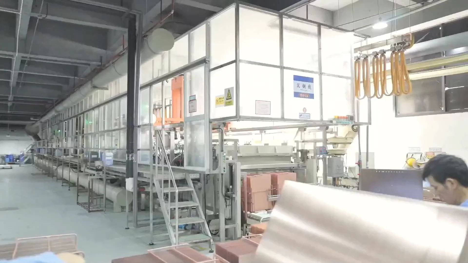
Hole preparation comes before the initial copper deposit. The equipment shown here represents a later metallization stage, not a direct view of desmear.
A chemical desmear route commonly conditions the resin, removes it with an oxidizing treatment, then rinses and neutralizes the panel before the next step. Plasma treatment instead uses reactive gases under controlled conditions to remove organic residue. Neither name guarantees a result by itself. The resin system, hole geometry and the selected process window determine whether the inner copper edge is adequately exposed without damaging the surrounding structure.
Etchback is not another word for cleaning. It deliberately removes some dielectric around an inner-layer connection to expose more copper. Whether etchback is required, and how much is permitted, belongs in the agreed build specification. An operator should not increase treatment simply because a microsection shows a questionable interface; the same image may also require review of drilling damage, bath condition or later copper deposition.
| Operation | Question it answers | What it does not prove |
|---|---|---|
| Post-drill cleaning | Were loose particles and process residues removed? | It does not establish that bonded resin smear is gone. |
| Desmear | Is the relevant inner copper edge free of resin? | It does not prove the later copper deposit is continuous. |
| Etchback | Was specified dielectric removal achieved at the connection? | It is not automatically required on every board. |
| Initial copper deposit | Did the prepared barrel receive conductive coverage? | It does not explain an earlier smear defect by itself. |
A standard multilayer through hole crosses the full board. A buried via is made within an inner-layer subassembly, while a blind via connects from an outside layer to one or more inner layers. Their treatment and inspection points therefore cannot be assumed to be identical. Small or deep features also need a review of how treatment reaches the wall and how the processed panel is handled before metallization.
The material matters just as much as the hole label. An FR-4 resin system, polyimide-based flex construction and a hybrid high-frequency laminate do not necessarily respond to the same treatment. That does not mean plasma is always better or a chemical route is always enough. The engineering team should use the actual stackup and laminate data to choose a qualified route. KnownPCB's high-frequency PCB service page describes plasma desmear for relevant RF builds; it should not be read as a promise that every order uses that process.
A microsection is useful when the question is whether an inner copper edge was properly exposed and connected to the plated barrel. The report should identify the hole, layer, sample position and production stage. If the sample was cut after plating, the inspector should describe both the interface and the copper coverage rather than treating every gap as a desmear failure.
Electrical testing answers a different question. It can reveal an open or short in the tested network, but a passing test does not display the local hole-wall interface. A representative section, process records and the agreed inspection plan are needed when a hidden interface defect is suspected. KnownPCB's PCB quality-management process provides the wider inspection context.
If one sampled hole shows residue, the first response is to identify its location and compare nearby holes from the same panel. If the pattern appears across a batch, the team should review drill condition, treatment controls and the time between preparation and deposition. A single microsection cannot establish the condition of every hole on the board.
Send the Gerber or ODB++ data, NC drill files, stackup, laminate specification, finished board thickness and finished-hole requirements. Mark blind, buried and filled vias separately. If a drawing specifies etchback, an unusual inner-layer connection or a special reliability test, include that requirement with its acceptance method. These details let the fabricator review the hole-preparation route before production rather than after a failed section.
For an existing defect, also provide the hole location, section image, sample orientation and the observed production lot. Do not send only a cropped photograph labeled "poor desmear." The same visible gap can call for checks at more than one stage of the process.
Request a hole-preparation and plating DFM review
No. Desmear targets resin left by drilling. Etchback intentionally removes a specified amount of dielectric around an inner-layer connection. The build specification determines whether etchback is required.
Yes. Electrical test checks the measured circuit path. It does not show every local interface inside the hole. A suspected smear condition needs location-specific inspection and process records.
No. The chosen method depends on the laminate, hole structure and qualified factory process. The result should be checked against the actual board requirements, not inferred from the process name.
July/10/2026Prototype PCB Assembly vs Low Volume PCB Assembly
May/27/2026DFM for PCB with Large-Footprint Components
June/24/2026High-current Heavy Copper PCB
March/20/2026Automotive Multi Camera System Demands and Challenges in PCB Process
September/24/2026PCB Hole Wall Roughness: Causes, Inspection and Plating Risks
