
A drilled hole can look clean at the entrance while resin still covers an inner-layer copper edge. Heat from drilling can soften resin, which the drill then drags across the exposed copper. If that film remains, the first copper deposit may sit on resin without making contact with the inner layer. The PCB desmear process removes this residue before hole metallization.
For holes that carry electrical connections in a bare PCB, a dark area in a cross-section needs investigation. When a connection is missing, we identify the hole and layer, then review the drilling, desmear, activation, and initial copper-deposition records in order. The image alone cannot tell us which step failed.
Table of contents
Mechanical drilling cuts through glass fiber, cured resin, and copper in succession. If the drill is worn, the cutting conditions are unsuitable, or an area becomes too hot, resin can form a thin film over the exposed edge of an inner copper layer. The finished hole may still meet the drawing's diameter requirement, but that film separates the copper surfaces that need to connect. The University of Maryland's CALCE note on resin smear describes this hole-wall and inner-copper interface defect.
Loose debris, resin smear, and hole-wall roughness are separate inspection findings:
For the mechanical wall condition, see KnownPCB's article on PCB hole-wall roughness and cross-section inspection.
A production report should identify the hole, affected inner layer, section direction, and inspection stage. Union Tool's resin-smearing evaluation method compares the width of resin seen at an inner copper edge with the thickness of that copper layer. The method helps describe a finding. It does not establish one acceptance number for every order.
Mechanical drilling comes before hole-wall cleaning. This production photo does not show resin smear inside an individual hole.
For a conventional plated through hole, the basic order is drilling, post-drill cleaning, desmear and any specified hole-wall treatment, activation, an initial conductive deposit, and copper electroplating. The route varies with the material and process. If resin still covers an inner copper edge before the first deposit, adding more barrel copper later cannot by itself restore that connection.
A through hole crosses the board. Blind and buried vias connect different layers and may be formed at different stages. A non-plated mounting hole does not require a continuous conductive barrel. When these hole types appear in one drill package, the inspector should confirm each type against the drill file and stackup before applying a plated-hole criterion. KnownPCB's PCB drilling quality article provides more context on the drilling stage and what follows it.
Desmear prepares the dielectric surface and exposed inner-layer interface for activation and the first copper deposit. If a section shows a missing connection at an inner copper edge, check that location for remaining resin. For a gap elsewhere on the barrel, also review activation, initial deposition, and later electroplating records.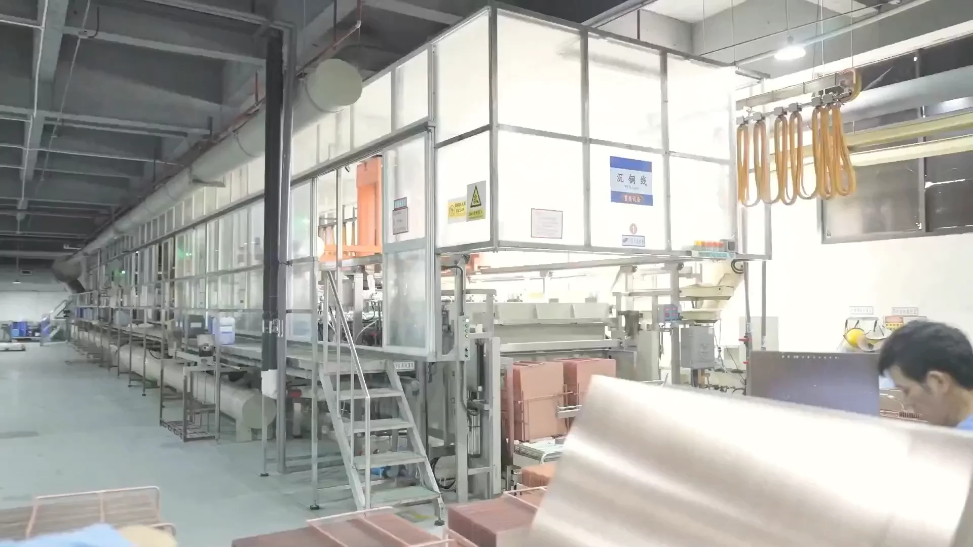
The initial copper deposit follows hole-wall preparation. This photo shows a later metallization stage, not a microscopic desmear defect.
In a common chemical route, the resin is conditioned, an oxidizing treatment removes residue, and the panel is then rinsed and neutralized. A plasma route uses controlled gases to treat organic residue. Both routes need to be checked against the actual laminate and hole structure. The process name alone does not prove that the inner copper edge has been exposed.
Etchback deliberately removes some dielectric around an inner-layer connection to expose more of the copper edge. The customer's drawing and agreed build requirements determine whether it is needed and how much removal is allowed. Before extending treatment time to address an abnormal section, check for drilling damage and later copper-deposition problems that could leave a similar gap.
| Stage | What to check |
|---|---|
| Post-drill cleaning | Were loose particles and process residues removed? |
| Desmear | Is resin still covering the relevant inner copper edge? |
| Specified etchback | Was the agreed dielectric removal achieved? |
| Initial copper deposition | Did the prepared hole wall receive continuous conductive coverage? |
Record these findings separately. A successful initial copper deposit does not replace the checks made earlier in the process.
A standard through hole spans the full PCB. A buried via may be completed in an inner-layer subassembly, while a blind via connects an outer layer to selected inner layers. The processing point, accessible hole wall, and inspection sample position therefore differ by hole type. For a small or deep hole, engineering also needs to check that treatment reaches the wall and that the hole is adequately rinsed before metallization.
FR-4, polyimide flex constructions, and hybrid high-frequency laminates may need different desmear conditions. Some can share a qualified route. To choose between chemical and plasma treatment, engineering needs the stackup, laminate data, and evidence that the process works on that construction. KnownPCB's high-frequency and high-speed PCB page provides material and process context.
In a cross-section, inspect the inner copper edge for residual resin and check its connection to the plated copper. Record the hole, layer, sample position, and production stage. For a sample taken after electroplating, describe the resin at the interface and the copper coverage separately. A report that labels every gap "insufficient desmear" gives the next engineer a diagnosis before the evidence supports it.
Electrical testing checks the tested network for opens and shorts under specified conditions. It does not reveal the physical cause of an open circuit or show every small interface inside a hole. When an interface defect is suspected, use the agreed cross-section sampling plan with production records and follow-up samples. KnownPCB's quality-management page describes its broader finished-board inspection approach.
If residue is found at one hole, first record where that hole sits on the panel. Then compare nearby holes and samples from the same lot. If the same condition recurs, review drill condition, desmear records, and the time between hole-wall preparation and initial copper deposition. One cross-section describes its sampled location, not every hole on the board.
Submit Gerber or ODB++ data, NC drill files, stackup, laminate specification, finished board thickness, and finished-hole requirements. Mark blind, buried, and filled vias separately. If the drawing requires etchback, an unusual inner-layer connection, or a reliability test, include its acceptance method. The fabricator can then review the hole-preparation route before production.
For an existing defect, include the hole location, original cross-section image, cut direction, and production lot. A cropped photo labeled "poor desmear" leaves the engineer without the information needed to trace the gap through production. To request an engineering review, submit the files through KnownPCB's contact page.
No. Desmear removes resin left by drilling. Etchback intentionally removes a specified amount of dielectric around an inner-layer connection when the order calls for it.
Yes. Electrical testing checks the tested circuit path. It does not show every copper-to-resin interface inside the hole. If the order calls for cross-sections or an interface defect is suspected, inspect samples and process records.
No. The treatment depends on the laminate, hole structure, and qualified factory process. Check the finished-board requirement and inspection result rather than assuming one method fits every board.
August/07/2026Guide to PCB Prototype Service and Prototype PCB Assembly
April/23/2026Through-Hole Assembly Capabilities & DFM Checklist

September/28/2026PCB Annular Ring Breakout: Causes, Layer Inspection, and DFM Checks
October/06/2026PCB Bow and Twist Measurement: How to Measure and Report Bare Boards
March/04/2026RFPCB Optimization for Ultrasound Probe Medical Devices
