
Telecom PCB manufacturing starts with a channel requirement and ends with an approved physical build. Between those points, the team must control the changes that affect a long high-speed route or an RF path: dielectric construction, copper configuration, launches and layer transitions. A board can meet a continuity test while the channel still lacks electrical margin.
The most useful manufacturing review follows one critical channel from connector to device. It identifies what fabrication can control, what must be checked in the electrical model and what evidence the trial build needs to provide. This article uses that route to organize the release of bare boards for telecom and networking equipment.
Follow the channel to release
A data-rate label alone is not a fabrication specification. Identify the interface, route length, layer assignment and relevant electrical requirements. For a digital link, the device and interface guidance determines which channel constraints matter. For an RF path, identify the operating band and the response being protected, such as loss or phase. Keep those definitions with the approved drawing.
Separate the bare board's deliverables from the assembled system's validation. The fabricator can build specified structures and provide agreed production records. Component packages, connectors, assembly and active equalization add other parts of the finished channel. Agree who owns the model and the final product test so that a bare-board inspection is not assigned a system-level claim it cannot support.
KnownPCB's telecom and high-speed computing page describes application constraints and manufacturing review areas. Use the individual channel and the required records to turn those areas into an order-specific fabrication request.
Begin where the signal enters the board or leaves a device footprint. Inspect the pad, escape route, reference plane and ground connections as a connected structure. Artwork compensation near a launch can have a different electrical effect from the same adjustment along a uniform trace. Mark regions where geometry changes require designer approval.
Use the connector or device supplier's current design data for the selected part. A footprint that matches the mechanical drawing does not automatically produce the intended electrical launch in a different stackup. Confirm the reference-plane spacing and the conditions assumed in any supplied model.
For the uniform route, verify the material system and the finished conductor dimensions used by the channel model. Include the copper option when loss is sensitive to its surface profile. An approved laminate grade with a different foil configuration can leave a model and a manufacturing order describing different conductors.
Rogers' technical paper on copper foils for high-frequency materials discusses how conductor profile affects loss and phase response. Use material-specific data for the proposed build rather than assigning one roughness assumption to every copper option.
The multilayer board below illustrates dense component escape and routed copper in a high-speed product. Its photograph does not disclose the channel model or establish any transmission-rate result.
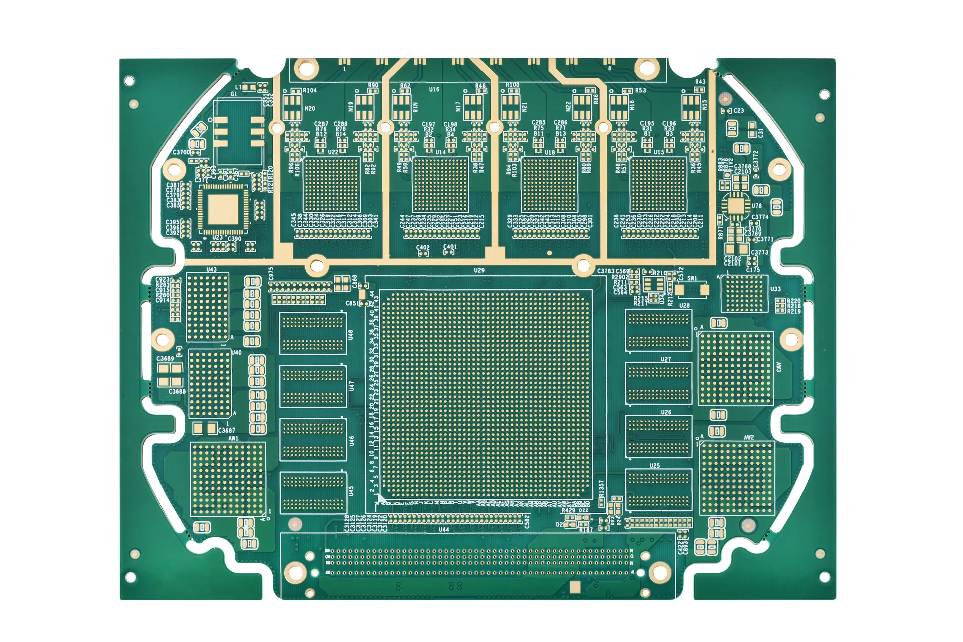
The multilayer product illustrates routing density; channel performance is established by the approved design and verification.
At each transition, identify the signal's entering and exiting layers, unused barrel and nearby return connections. Review the pad and clearance geometry on traversed planes. The relevant structure extends beyond the drilled hole itself.
Texas Instruments' High-Speed Interface Layout Guidelines discusses via discontinuities, backdrilling and reference paths. Its recommendations belong to their stated application context. Use the selected interface and channel analysis to establish the residual-stub requirement for your design.
If backdrilling is required, give the manufacturer the affected hole list, drilling side, stop layer, relevant clearances and residual requirement. Resolve how the stop is defined and how it will be inspected. A generic “backdrill high-speed vias” note leaves room for different interpretations of which vias and layers are involved.
KnownPCB's via-stub and backdrilling case gives related manufacturing context. The telecom release should reference the exact transition geometry being approved rather than repeat a general backdrilling overview.
The mechanical-drilling photograph below shows production equipment only. It does not show a controlled-depth backdrilling operation or verify a residual-stub dimension.
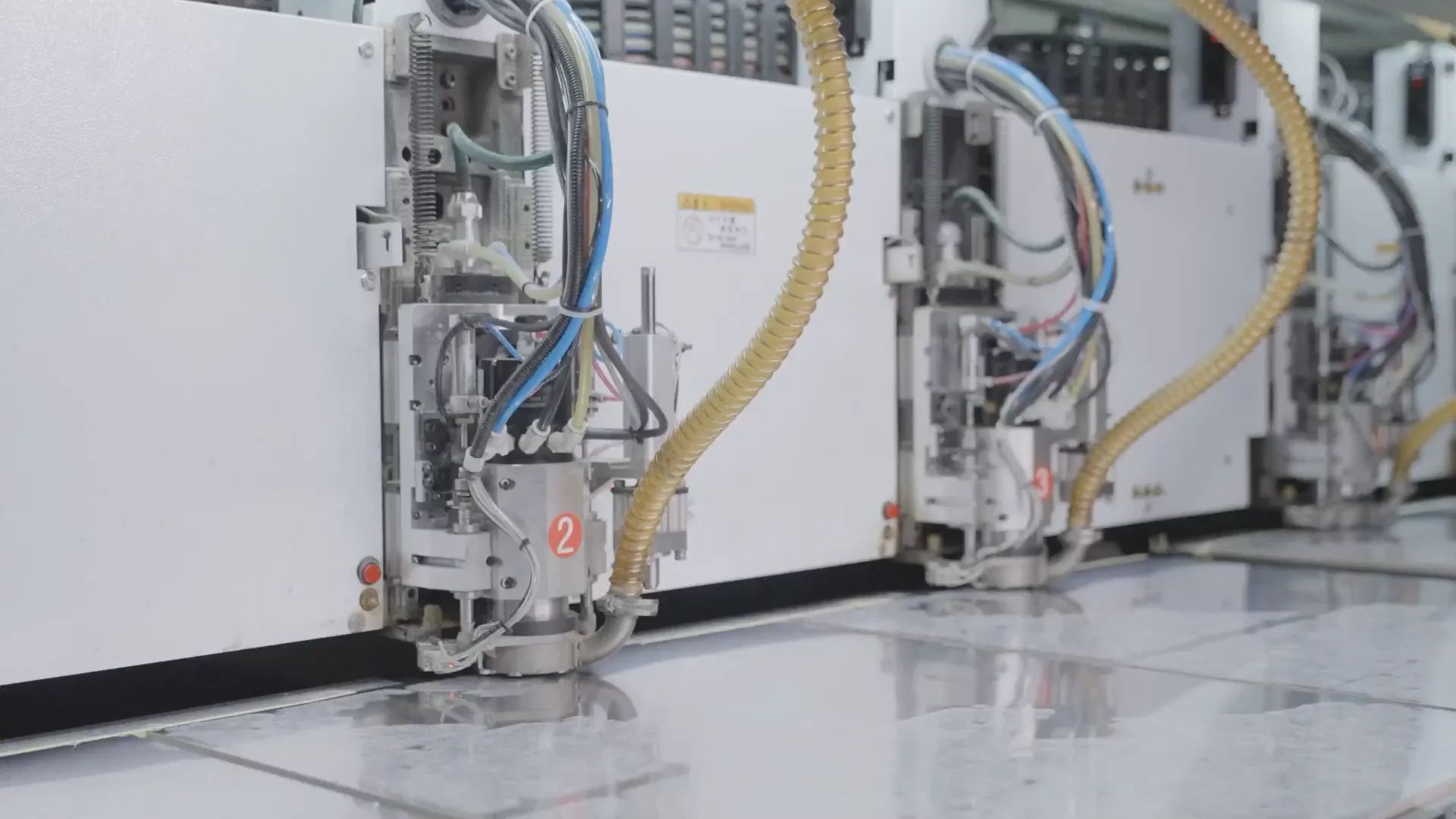
Mechanical drilling equipment is shown as process context, without implying a measured backdrill result.
Build the trial plan around the uncertainty that remains after the design review. If dielectric spacing is the concern, a representative physical measurement can test the construction. If the risk is the routed channel's loss, agree the appropriate electrical structure and frequency-domain evidence. If it is a via transition, choose a structure that includes that transition.
Impedance coupons are useful production evidence for the structures they represent. Their acceptance does not demonstrate the full channel's insertion loss or the performance of every launch. Put the different evidence requests in separate lines of the quotation so scope and responsibility remain visible.
Preserve trial conditions when comparing results. Record artwork and stackup revisions, material construction, panel or coupon identity and relevant measurement settings. If a board is changed after the trial, identify which evidence still applies and which needs to be repeated. A changed layer pair or launch can invalidate a comparison even when the top-level product name stays the same.
The release package should name the approved stackup, impedance structures, material and copper restrictions, controlled artwork regions and special drill requirements. Connect those documents with one revision or release identifier. Purchasing and the factory should be able to resolve a question without reconstructing a chain of attachments.
Set a change-notification rule for replacements in laminate, foil, bonding system or agreed process that can affect the approved build. A repeat order should carry forward the evidence scope, including any trial limitations. If the supplier proposes a change, return to the affected section of the channel rather than reopening unrelated parts of the entire design.
The RF and high-speed PCB manufacturing service supports the next engineering discussion. Request a telecom bare-board manufacturing review with the channel constraints, stackup and special drill data. Ask the response to identify proposed changes and the records included with the first lot.
July/10/2026Prototype PCB Assembly vs Low Volume PCB Assembly
September/28/2026PCB Plating Voids in Through Holes: Causes, Evidence and Prevention
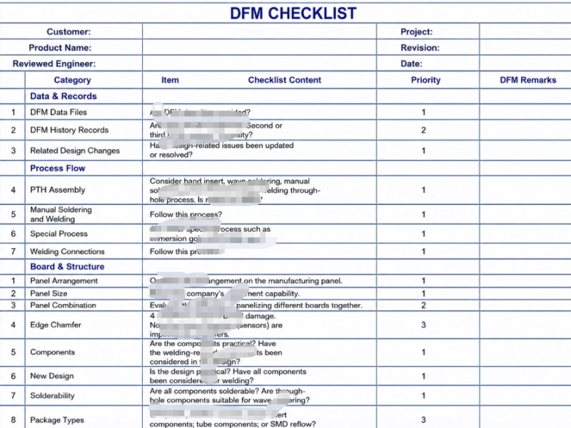
May/27/2026DFM for PCB with Large-Footprint Components
March/04/2026RFPCB Optimization for Ultrasound Probe Medical Devices
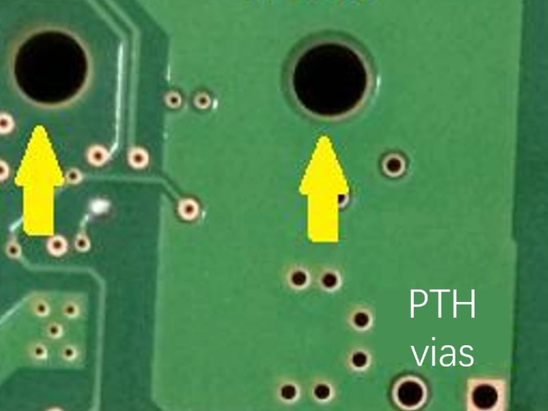
April/23/2026Through-Hole Assembly Capabilities & DFM Checklist