
Medical sensor PCB design begins with the signal at the connector and the disturbances that can change it before conversion. A board for a small optical signal needs different routing decisions from one carrying a digital sensor interface. Specify the measurement path first, then decide which parts of the board need guarding, a continuous reference plane, or mechanical protection.
For a bare-board order, that work must survive the transfer into manufacturing data. A guard clearance, an isolated copper region, or a flex boundary can disappear when it exists only in a layout engineer's notes. The release package should identify which features affect the measurement and which changes require approval.
Follow the measurement path
Identify the sensor output type on the drawing. A photodiode feeding a current-to-voltage amplifier is sensitive to current entering through unwanted leakage paths. An electrode input has its own bias network and protection requirements. A digital sensor's clock and supply currents require a different review. Calling all of these nets "low noise" leaves the fabricator without a useful distinction.
For a high-impedance input, review nearby conductors on every copper layer. A narrow input trace may have a power pour beside it, a test pad above it, or an internal plane beneath it. Those relationships are easy to miss when the review uses only a top-side screenshot. Include a layer-by-layer view around the sensitive node and identify any copper removal that the circuit designer requires.
Analog Devices describes how board leakage can alter a photodiode amplifier and how a driven guard can reduce leakage into its input. The photodiode circuit design reference also shows why guard potential must follow the node being protected. A grounded copper ring and a driven guard are different circuit choices.
State the intended guard net and its clearance from the input copper. If the circuit calls for an exposed guard or a solder-mask opening, include it in the manufacturing layers. The board house should ask before adding copper or changing mask in that region. Any request for a special cleanliness check also needs a defined method and acceptance condition agreed before fabrication.
Consider access during evaluation. Adding a large test pad to the highest-impedance point changes the physical node. A nearby digital test connector can introduce another coupling path. Let the circuit designer choose where measurements will be taken, and preserve those decisions through the fabrication review.
Trace a complete signal route with its return connection. Locate the analog front end, its reference connection, the local supply bypass connections, and the route back to the sensor connector. Then examine whether a radio, display interface, or switching supply uses the same narrow copper connection. Placement and current paths need to be checked together.
Texas Instruments gives device-specific layout guidance in the ADS1292R data sheet, section 11. It calls for short analog connections, supply bypassing close to the device, and digital return paths arranged away from the analog return path. Use the guidance for the selected front end rather than applying a single grounding pattern to every medical sensor.
A split plane deserves a routing review of its own. If a clock or data trace crosses the split, its return current must find another path. Review the reference beneath the trace at each layer change. Keep safety isolation boundaries intact, and let the system engineer define how functional references connect on either side of those boundaries.
List controlled-impedance nets only where the circuit requires them. A low-frequency electrode input and a fast digital connection do not automatically need the same impedance rule. For the latter, name the layer, target value, and reference construction. For the former, the input leakage and shielding requirements may deserve more attention than a nominal transmission-line impedance.
A sensor board often connects to a housing, cable, or flexible tail. Put those interfaces in the review before routing is frozen. A connector placed for a clean electrical path may sit where a mounting screw or cable bend loads the board. Show the mounted condition as well as the flat board outline.
When the design uses flex, distinguish a bend made during installation from motion repeated during service. Provide the intended bend region and the assembled shape. The chosen copper construction and finished flex thickness must be assessed against those conditions. A drawing that shows a folded tail without a defined bend region leaves its mechanical use open to interpretation.
A flexible circuit panel illustrates the kind of interconnect geometry that may need mechanical review. The pictured board is a general manufacturing example; its photograph does not identify a medical application or establish a tested bend life.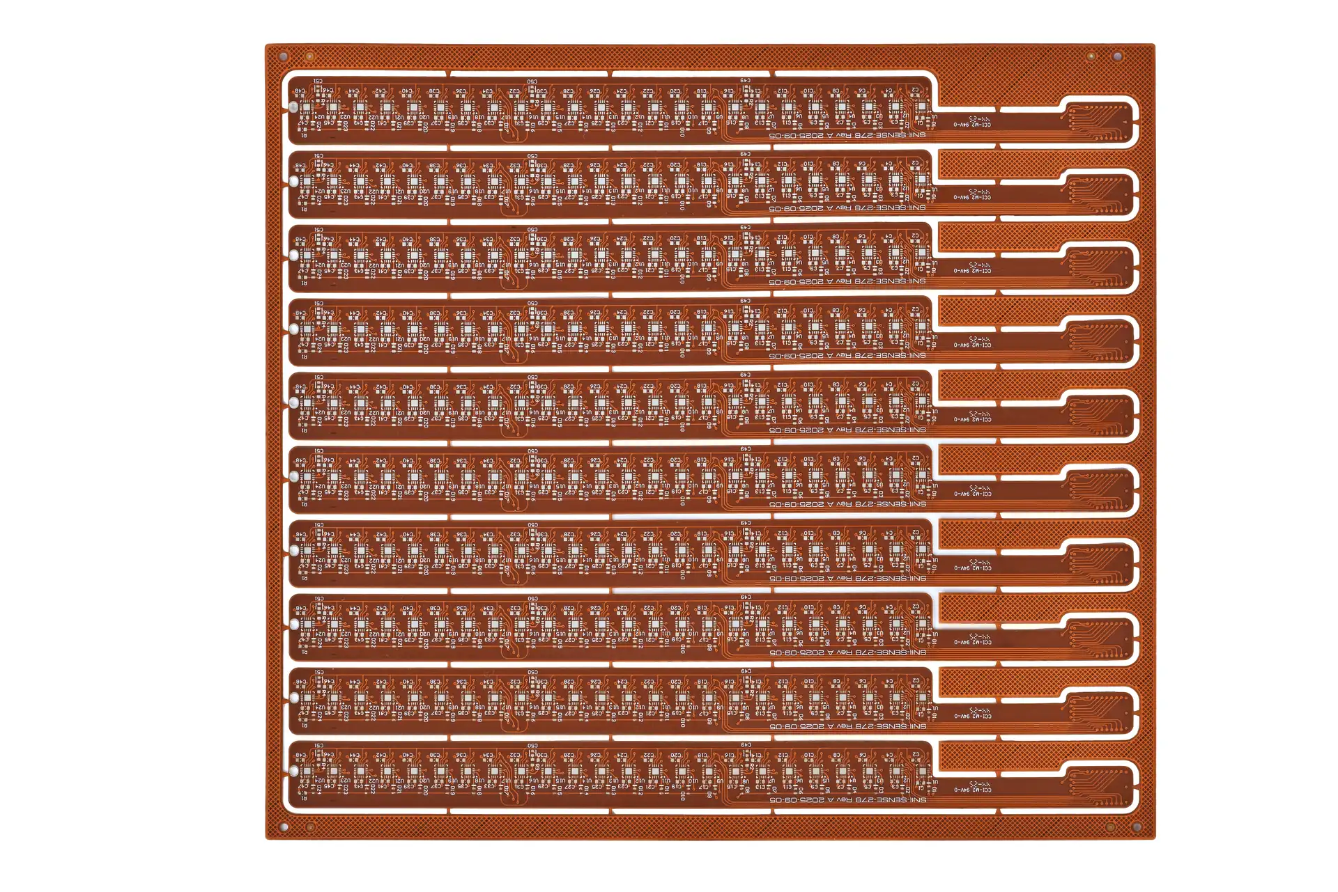
This flexible circuit panel illustrates interconnect geometry; it does not document a medical device or a bend-life test.
For a rigid-flex implementation, coordinate the rigid outline and coverlay termination with the mechanical drawing. Keep the transition location consistent across the stackup and fabrication files. KnownPCB's rigid-flex PCB manufacturing scope is the starting point for reviewing the construction, while the medical electronics application page outlines the broader application requirements.
Keep enclosure exposure in the requirements too. An internal circuit, a skin-contact assembly, and a device intended for cleaning or sterilization have different material-review needs. Specify the exposure for the complete product. A laminate name or surface finish alone cannot establish suitability for those uses.
The first article should be traceable to a defined fabrication revision. Include the approved stackup and material designations, and identify sensitive regions in the notes. If the supplier proposes a substitute laminate, a different copper construction, or a mask adjustment, request an engineering assessment before accepting the change. Preserve the approved response with the released package.
Match each requested inspection to what it can establish. Bare-board electrical testing checks connectivity and isolation under the agreed test conditions. It does not establish sensor accuracy or confirm operation in the finished enclosure. A dimensional record can document a connector datum; a board photograph cannot substitute for that measurement.
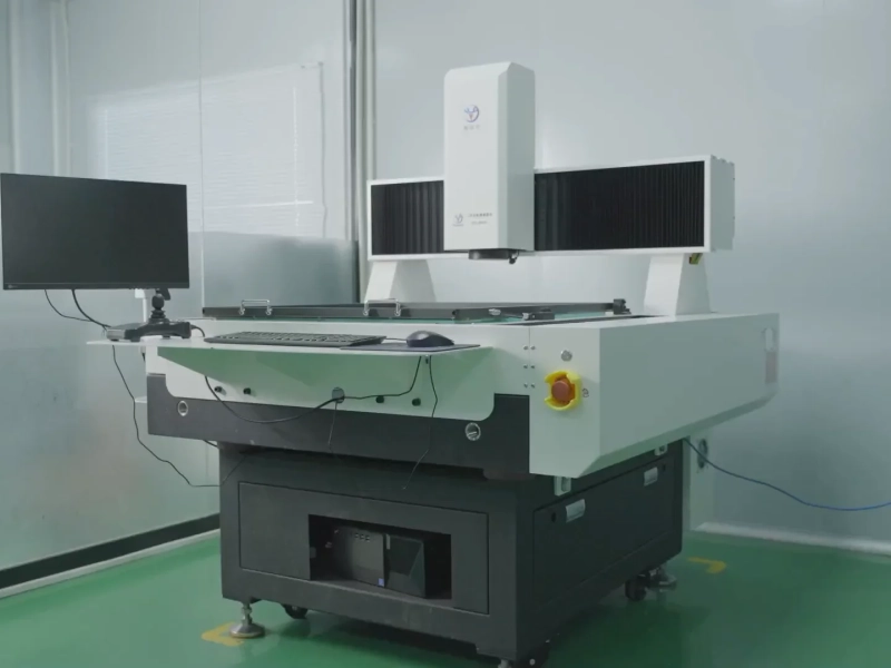
The test equipment shown here provides manufacturing context for bare-board connectivity inspection. The photograph contains no evidence of a clinical test, sensor calibration, or medical device approval.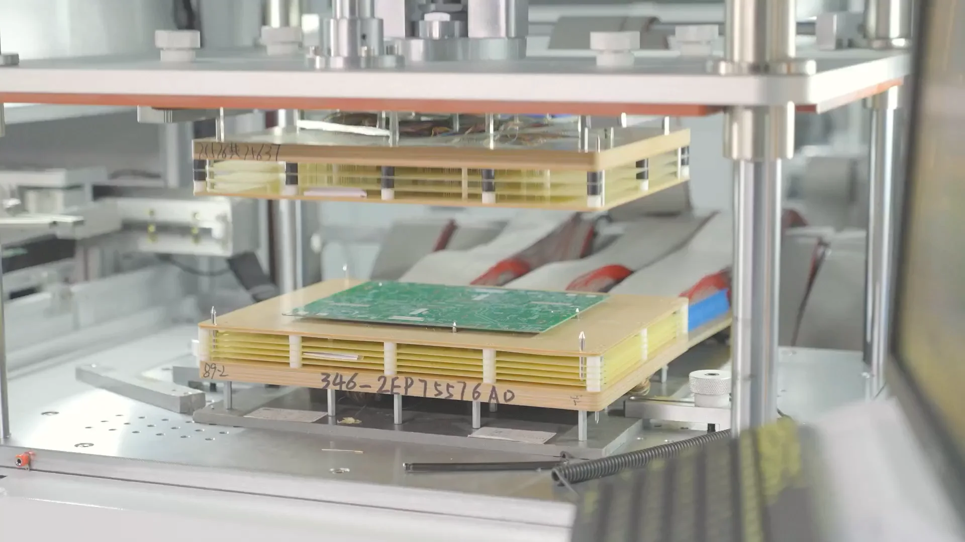
Bare-board electrical testing supports connectivity checks; it does not measure sensor accuracy or device safety.
Agree which lot records will accompany the order and how they relate to the board marking. Link the material record, approved deviation, and inspection result to the same revision. If an assembly later drifts during a humidity test, that link helps the team identify which boards and manufacturing decisions belong in the investigation.
KnownPCB's quality-management page describes the general inspection framework. Specify project-specific evidence before ordering. The device manufacturer must still establish the applicable product requirements and verify the finished system; a PCB inspection class or supplier quality statement does not replace that work.
Send the fabrication package and mechanical constraints through the KnownPCB engineering contact page. Mark the input regions that require approval before modification, and name the evidence needed for repeat orders. That gives the fabricator a defined board to build and gives the design team a controlled basis for comparing later lots.
October/06/2026PCB Bow and Twist Measurement: How to Measure and Report Bare Boards
September/28/2026PCB Annular Ring Breakout: Causes, Layer Inspection, and DFM Checks
October/22/2026RF PCB Supplier Evaluation: Check the Build Evidence
March/24/2026HDI Microvia Cracking | Failure Analysis Steps

May/15/2026MOSFETs and SMT Integration