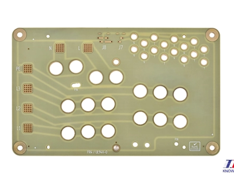
An EV inverter gate driver PCB can sit beside a power module and still have a long electrical gate loop. The outgoing gate trace may be short, while the return travels through a connector, a shared source conductor, or a distant plane connection. The complete outgoing-and-return path determines the geometry.
Begin a review at the driver output and follow the current back to its local supply. Then review the barrier that separates the control domain from the switching domain. These two views expose different problems and give the board fabricator specific geometry to preserve.
Contents
The power commutation loop carries energy between the DC-link capacitor and the switching devices. The gate loop charges and discharges the power device’s gate. Both influence switching behaviour, but they are different circuits. Enlarging the traction-current copper does not automatically improve the gate-return route.
Trace the driver output through the gate resistor and package connection, then return through the intended source or emitter reference to the driver. Include connector pins, vias, and package terminals. A route that looks short on one PCB can contain most of its inductance in the interconnect to a separate module.
Where the power device provides a Kelvin source or emitter terminal, its purpose is to give the gate drive a reference separated from the main current path. Preserve that relationship in the schematic, connector assignment, and copper. Rejoining it to the power return at a convenient point can defeat the intended separation.
The layout section of the Texas Instruments UCC21750-Q1 datasheet discusses proximity to the power device, local decoupling, and the Kelvin reference. These are device-specific instructions. Check the selected driver and power module documentation together, including any distinction between high-side and low-side reference planes.
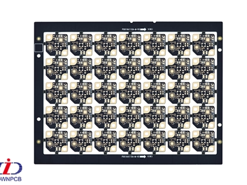
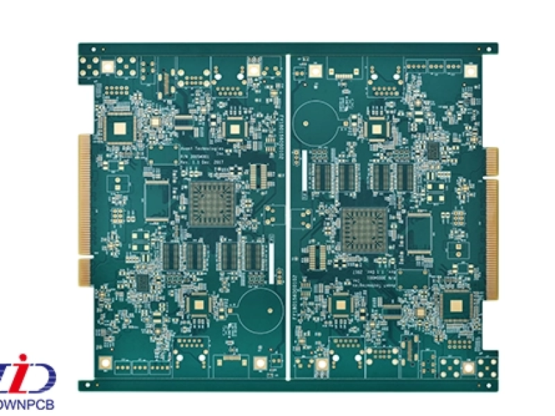
The bare-board example below shows large conductor areas beside fine lands and routed openings. It provides fabrication context only; it is not an identified EV gate-driver design or evidence that a particular loop inductance has been achieved.
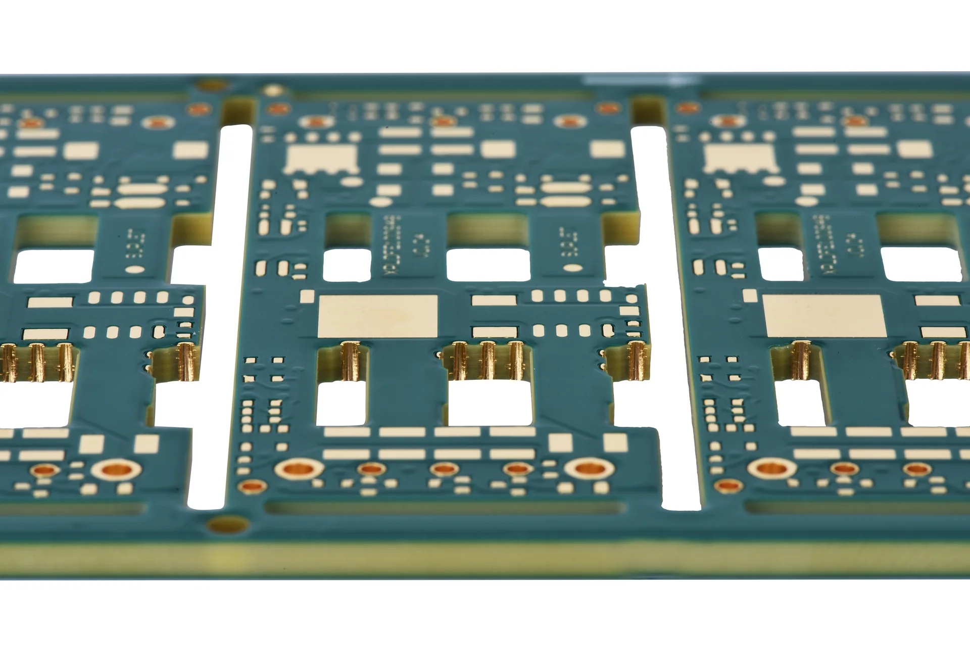
This bare-board example shows mixed large and small features; it is not evidence of a qualified EV gate-driver design.
The driver draws short current pulses during switching. Its local bias capacitors need a route to the supply pins and the corresponding reference that keeps the high-frequency current close to the driver. A nearby capacitor with a long return trace can perform poorly even though its placement looks satisfactory.
Review the supply-and-return loop on the actual layer pair. If a capacitor and driver are on opposite sides, include the via transition. Avoid routing a supply connection around an isolation slot and returning through an unrelated plane. The energy path should be understandable without assuming that every polygon labelled ground is equivalent.
Separate the references for input-side logic and output-side gate drive according to the isolation architecture. A reference plane on the control side must remain within its electrical domain. An isolated output domain may move rapidly with the switch node, so its copper area also affects coupling to nearby structures.
Protection and measurement returns require a specific review. Desaturation sensing, an active clamp, and local voltage monitoring can share the driver’s environment while remaining sensitive to the gate-current pulse. Follow the component manufacturer’s routing arrangement instead of connecting all returns to the nearest available copper.
These choices belong in the approved layout and stackup. The fabricator should receive clear instructions about keepouts and controlled features, while the circuit designer validates the resulting waveforms with an appropriate measurement setup. The fabrication drawing alone does not predict the switching transient.
Mark which copper belongs to the controller, each floating driver output, and any chassis-connected feature. Review outer layers, internal planes, vias, mounting hardware, and connector pins. An empty strip on the top layer does not establish a barrier if a plane crosses underneath it.
The required separation comes from the electrical design and the applicable product evaluation, including working voltage, transient stress, environment, and material properties. Do not adopt one distance from an unrelated inverter or assume a gate-driver package rating qualifies the complete PCB.
A routed slot may be part of the construction, but its ends, finished dimensions, and copper relationship must be defined. Consider mechanical support around the slot, component bodies bridging it, and possible contamination paths in the enclosure. It also changes routing space for local returns.
TI’s automotive dual-channel SiC gate-driver reference design provides a concrete reference implementation and layout discussion. Use its circuit boundaries and design files to understand the review method. Its achieved performance and construction are not automatic ratings for a newly routed board.
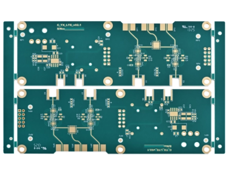
The routed-panel photograph below illustrates machining features only. Neither the photograph nor the presence of a slot establishes a creepage requirement, partial-discharge result, or dielectric-withstand rating.
Review connectors, measurement access, and the release drawing
A connector is part of the gate loop when the driver and module are separate. Check adjacent pin functions, the return assignment, and how the pair enters the board. A cable or mezzanine connection can add loop area, and mechanical placement can make the two conductors separate farther than expected.
Test access needs the same attention. A long gate test trace can become a branch that changes the circuit being observed. Define where the validation team will probe and how the reference connects. Keep any permanent measurement feature consistent with the intended switching behaviour and isolation geometry.
The existing power-supply PCB article covers broader power-board considerations. This review stays with the local gate-drive path and the barrier. The KnownPCB energy and power-electronics page provides the manufacturing enquiry route for discussing stackup, copper, drilling, and routed features.
Release the actual layer stack, finished copper definition, drill files, slot drawing, netlist, and barrier keepouts together. Identify any region where a proposed CAM change needs circuit-designer approval. A copper pour adjustment that seems harmless for fabrication can change the driver’s reference or coupling.
Agree which fabrication records will be supplied and which switching, insulation, and system tests remain with the product team or an approved test party. Ordinary board continuity testing cannot establish gate-waveform quality or qualify an automotive inverter. Material selection and board manufacture are inputs to that validation, not substitutes for it.
When a prototype changes, retain the reason beside the revision. For example, distinguish a gate-return reroute from a slot adjustment or a bias-decoupling change. This makes later waveform comparisons useful because the team knows which physical condition was changed.
Submit the module interface, domain map, and fabrication files for an EV gate-driver PCB manufacturability review. Include the controlled return and barrier features. The resulting discussion can then resolve buildable geometry without assigning unverified performance or qualification claims to the board.