
Blog & Design Guide

An HDI skip via is a blind connection that bypasses at least one intervening copper layer. For example, a via defined from L1 to L3 reaches the target at L3 while passing L2 without connecting to it. That is a different structure from an L1–L2 microvia, and it carries a different clearance and fabrication review. Define the start layer, target layer, skipped layer, dielectric span, and construction in the released data before asking the supplier to confirm feasibility.
Example layer-pair record · hypothetical labels only
Via ID — V1
Start layer — L1
Target layer — L3
Intermediate layer crossed — L2
Electrical connection to L2 — None
Construction — To be confirmed by the fabricator
In this example, L2 still needs copper clearance where the drill or via barrel passes through it. It has no electrical land connection to V1. The labels do not specify dielectric thickness, hole size, drilling method, or whether this layer span can be made in the proposed board.
On this page: Read the layer-pair record · Distinguish the via structure · Check skipped-layer clearance · Release a reviewable drawing package
A layer span should identify where the via begins and where its conductive barrel must end. For an HDI skip via, also name each copper layer the bore crosses. This lets the fabricator map the transition to the stackup and review the dielectric sections that it must span.
Altium's via-type documentation defines a skip microvia by its nonadjacent layer span and identifies the first and last layers in its via definition. The drill outputs also associate microvia data with layer pairs. Use the stackup layer names consistently in the via properties, drill table, fabrication drawing, and any supplied layer-span list.
For the hypothetical V1 entry above, the layer path is L1 to L3 and L2 is traversed without a connection. The fabricator still needs the actual approved stackup to know what material lies between those endpoints. A number such as “second order” or “two-step HDI” does not replace the named layer pair because shorthand can vary between design and fabrication documents.
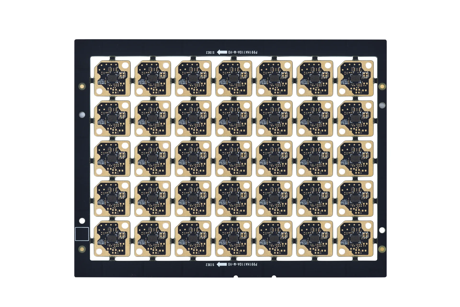
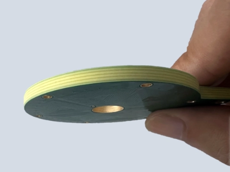
High-density PCB panel with fine-pitch component lands.
A blind microvia typically connects an outer layer to the next copper layer in the build-up. A skip via reaches a nonadjacent target and bypasses one or more copper layers. Two microvias that meet at an intermediate landing pad form a stacked connection, but that intermediate copper interface is electrically part of the route. Keep the geometry and electrical purpose explicit when sharing the stackup.
The chosen structure affects how the build is assembled and which layers are drilled at each stage. Altium's overview of skip vias and blind vias in HDI builds describes that a skip via bypasses the adjacent layer and requires the layout to reflect that nonadjacent span. It does not establish a universal drill depth or a particular factory's stackup support.
Use one agreed term for each via family in the data set. If a board contains adjacent blind microvias, stacked microvias, and a skip span, give them different IDs in the via table. That prevents a CAM reviewer from interpreting two similar-looking transitions as the same drill pair.

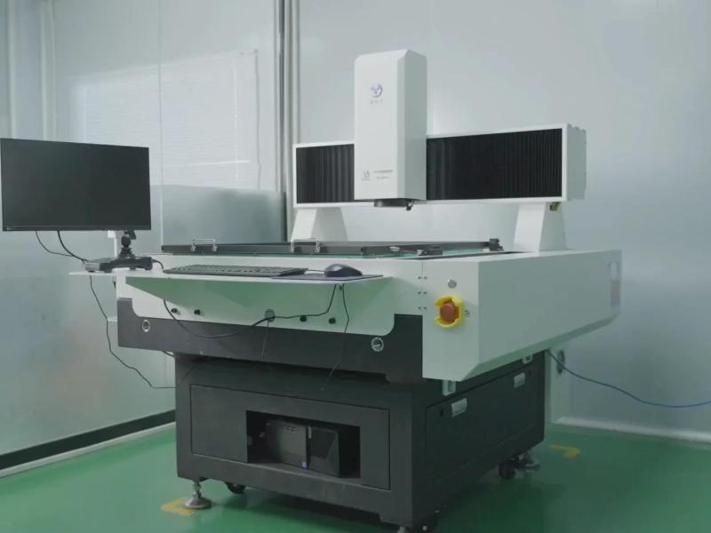
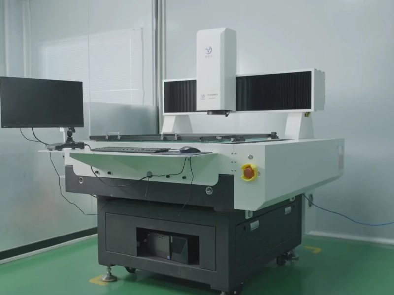
Laser-drilling equipment and an operator in a PCB production area.
When the via passes through an intermediate copper layer without connecting to it, the copper pattern must provide the required opening around the via. Review the skipped layer together with neighboring traces, plane openings, nearby capture pads, and the via center. A clearance drawn around a nominal center is only one part of the check; the fabricator also needs the defined via diameter and its applicable registration condition.
Make the artwork, drill or laser layer-pair outputs, and via schedule agree. A layer named “L2 clear” should match the actual copper artwork and the corresponding via location. If the design uses a plane on L2, include its antipad or keepout in the file that represents that layer. Do not rely on a note alone when the CAD data leaves continuous copper beneath the hole.
The public KnownPCB HDI fabrication page lists skip via among its HDI structures. The exact layer span and construction still need engineering confirmation for the submitted board. Avoid converting a general structure label into a promise that every proposed diameter, dielectric span, and stack sequence is available.

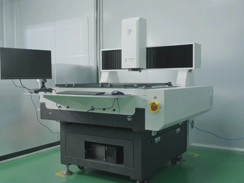
X-ray drill-targeting equipment in a PCB production area.
Submit the current copper artwork, drill and laser files, stackup, via table, board outline, and fabrication notes under one revision. Mark the skip via ID and its start and target layers. Identify the intermediate copper layers that the via crosses, the clearance around the via on those layers, and the material construction. Ask the fabricator to respond against that same layer pair and revision.
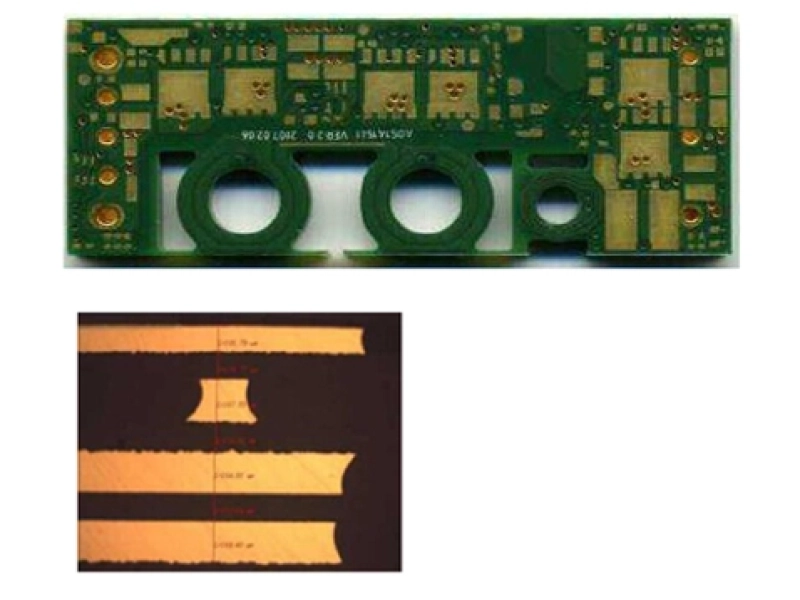
A cross-section can show the selected cut through the manufactured build, but a single section does not document every location around the board. If acceptance depends on the continuity or registration of a particular layer pair, state the sample location, layer identification, method, and drawing requirement before release.
For broad layer-build decisions, see the HDI stackup selection article. For fundamental through, blind, and buried via terms, see the via-type definition article. Send the updated stackup and named skip-via spans with the design through KnownPCB's contact page for a board-specific review.
October/30/2026IPC Class 2 vs Class 3: Does Your 4-layer PCB Need a Redesign?
April/29/2026Key Perspectives for Industrial-grade PCB
October/10/2026DC-DC Converter PCB Layout: Paths, Thermal Vias and Noise
April/16/2026High-Current Heavy Copper Design & Manufacturability
November/05/2026How to Improve HDI PCB Stackup Manufacturability Before Production?
Proven by 7 industries, 4000+ customer projects
Please contact us at sales@knownpcb.com, ask for engineering support here or use the form below to reach out to KnownPCB | Request a Manufacturing QuoteInclude your quantity, target delivery date and key requirements. File handling and NDA information. |