
Blog & Design Guide

Choose an RF PCB surface finish by identifying where it will cover the circuit. A long exposed transmission line, a short solder land and a board held in storage place different demands on the finish. Electroless nickel immersion gold (ENIG) and immersion silver can both provide solderable surfaces. To compare their RF effect, first locate the exposed copper and decide which part of the signal path must meet the loss budget.
Which length of conductor receives the finish?
Review the solder mask and the top copper together. An exposed RF feed can carry the surface finish for a substantial part of its length. ENIG places an immersion gold layer over electroless nickel. Immersion silver deposits silver on the exposed copper without that ENIG nickel layer. At higher frequencies, conductor current is concentrated toward the surface. The materials and thicknesses near that surface can affect conductor loss, alongside the original copper surface and trace geometry.
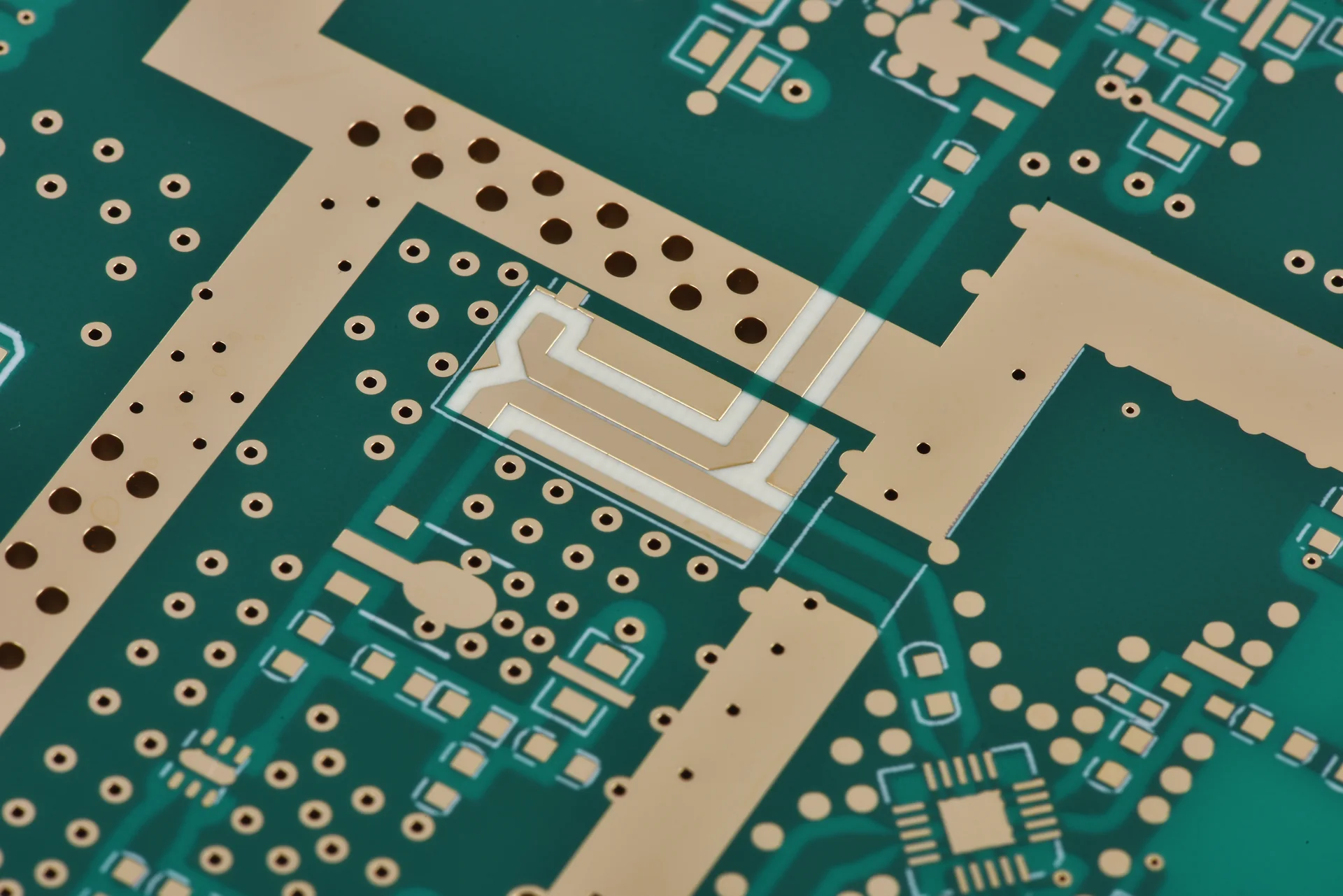
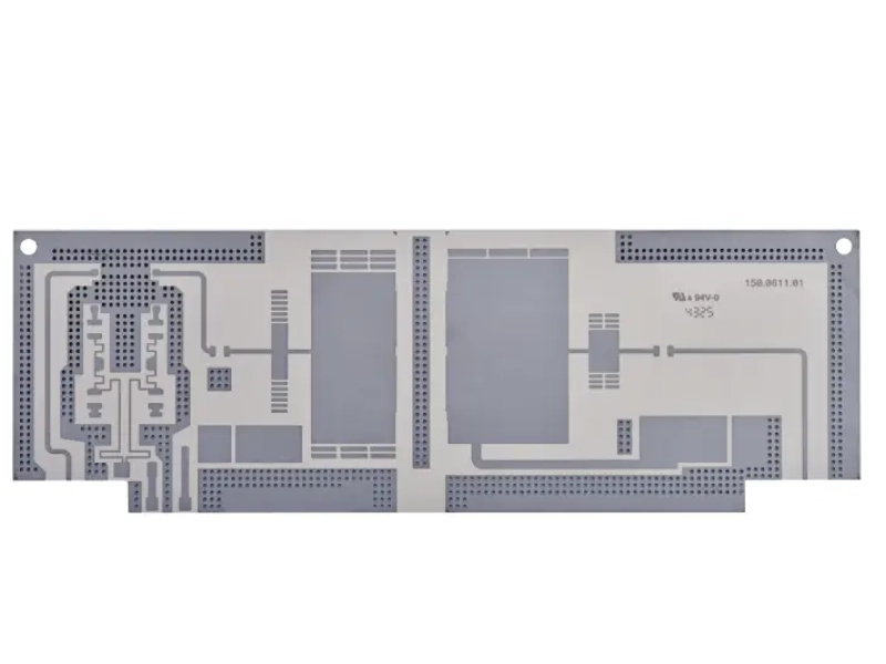
Exposed conductors and the surrounding solder-mask boundary on an RF board.
The useful comparison holds the transmission structure constant. Record the line length, stackup, mask coverage, copper profile, finish and operating band. If the result comes from a test, record which transitions were included and how the two coupons were measured. An Altium discussion of nickel-bearing finishes and RF loss explains why nickel-free finishes merit consideration. For a design with little margin, ask for geometry-specific evidence before assigning either finish a loss value.
Comparing two reports. Check whether their reference planes include the connector launch and whether the traces have the same length. If one result includes a connector pair and the other ends at the line, the difference includes the launch. If the copper foil or dielectric changed along with the finish, put those changes in the comparison record. A frequency sweep with matching structures helps the team evaluate whether the result applies to the intended board.
Where does the exposed land meet the transmission line?
A buried transmission line can run through the board without receiving the outer surface finish. Its transition through a via or surface pad still needs attention. On an outer layer, a mask opening around a launch or package land can expose a short trace segment as well as the pad itself. Mark the actual boundary in the fabrication data. A finish name on the drawing does not describe that boundary.
For a soldered package, check the package guidance and the assembler’s handling and reflow requirements. Analog Devices’ SMT land and surface-finish guidance lists several finishes used for leaded packages. Where a specific package application note calls for a finish and land pattern, bring that requirement into the drawing review. If a proposed finish changes the solderable land construction, clear it with assembly as well as RF engineering.
On a board with both an exposed antenna feed and ordinary solder lands, put the two requirements on the same review sheet. The RF engineer can identify the exposed feed and any sensitivity to added loss. Assembly can identify the package or land requirements that affect solderability. If those requirements point toward a selective finish, confirm whether that construction can be manufactured and inspected before adding it to the release notes.
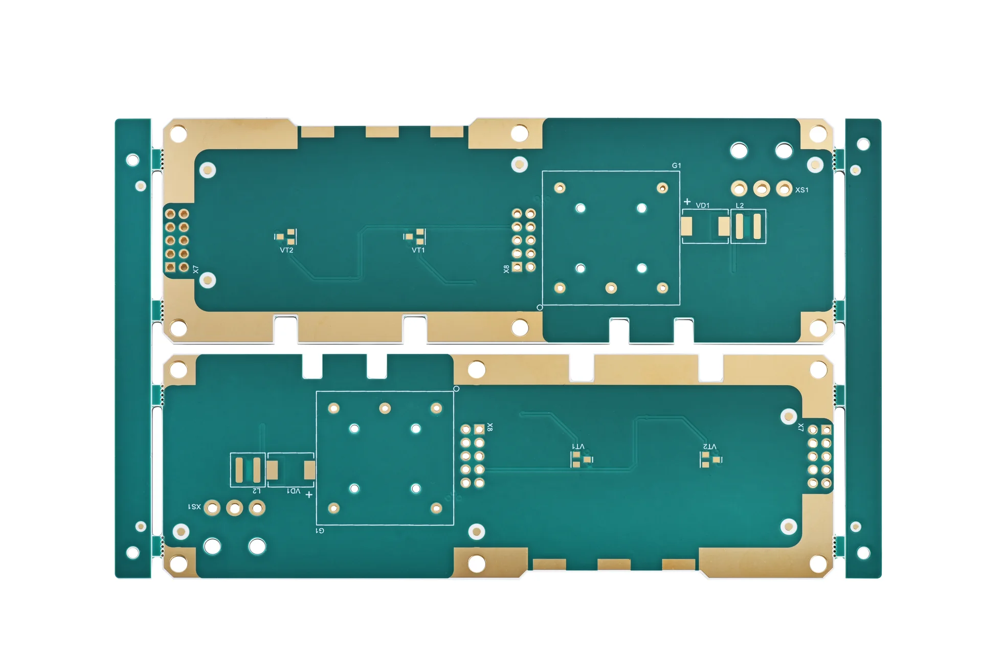
Solder lands and plated holes on a bare RF PCB panel.
How will the boards be packaged, opened and stored?
Immersion silver can tarnish after environmental exposure. Ask the fabricator for the packaging, handling and storage instructions for its process. Agree how long boards may wait unopened, what conditions apply once the package is opened and how any visible change will be assessed before soldering. A statement about an unopened shipment does not answer how an open lot will be handled on the production floor.
ENIG also needs an agreed finish specification and inspection plan. If the procurement document names a governing standard, record its revision and any finish thickness, lot report or acceptance details that apply to the design. Altium’s surface-finish descriptions in the fabrication process discuss ENIG and silver as different processes. Use the qualified process and the order requirements to agree the actual evidence.

PCB packaging station on the production floor.
Identify the finish on the drawing and note where a local requirement applies. Include the affected layer, mask openings, assembly lands and any exposed RF length. If the design needs a comparative loss result, define the coupon geometry, frequency band and acceptance limit before fabrication. The copper-roughness and skin-depth discussion covers another contributor to conductor loss. Keep its input separate from the surface finish in a comparison.
Use the approved finish name consistently in the fabrication notes, purchase order and inspection request. If a substitution is proposed because of schedule or availability, ask for its effect on the exposed line, the solder lands and storage conditions. Put the agreed decision on the same drawing revision that will be used to fabricate the board.
For a board with an unusual combination of launch geometry, exposed conductor and finish, send the stackup and mask data for RF PCB fabrication review. The general PCB finish overview is a starting point for the assembly and procurement terms that accompany the RF requirements.
May/12/20266 FPC Design Details to Prevent Assembly Failures
October/10/2026DC-DC Converter PCB Layout: Paths, Thermal Vias and Noise

September/06/2026High Current PCB Design: Current Paths, Copper, Vias & Thermal Limits
July/03/2026Single Sided PCB Board: How to Design and Purchase
October/09/2026ENIG Nickel and Gold Thickness: Drawings, XRF, and Reports
Proven by 7 industries, 4000+ customer projects
Please contact us at sales@knownpcb.com, ask for engineering support here or use the form below to reach out to KnownPCB | Request a Manufacturing QuoteInclude your quantity, target delivery date and key requirements. File handling and NDA information. |