
Blog & Design Guide

An RF PCB connector launch is the transition from the coaxial connector to the board’s transmission line and return path. For a board-edge mount, confirm the connector drawing, local board thickness, routed edge and copper registration together. A launch can fit mechanically and still introduce an RF discontinuity if the center pin or ground contact lands outside the intended geometry.
Drawing fields · Part number, drawing revision, mounting orientation, thickness range.
Use the selected connector’s mechanical drawing as the fit reference. Record which board face receives the center contact and where the body sits against the finished edge. For a clamp or board straddle, verify the allowed thickness at that location. Make the tolerance basis explicit when local copper, mask or finish affects the surfaces that contact the hardware.
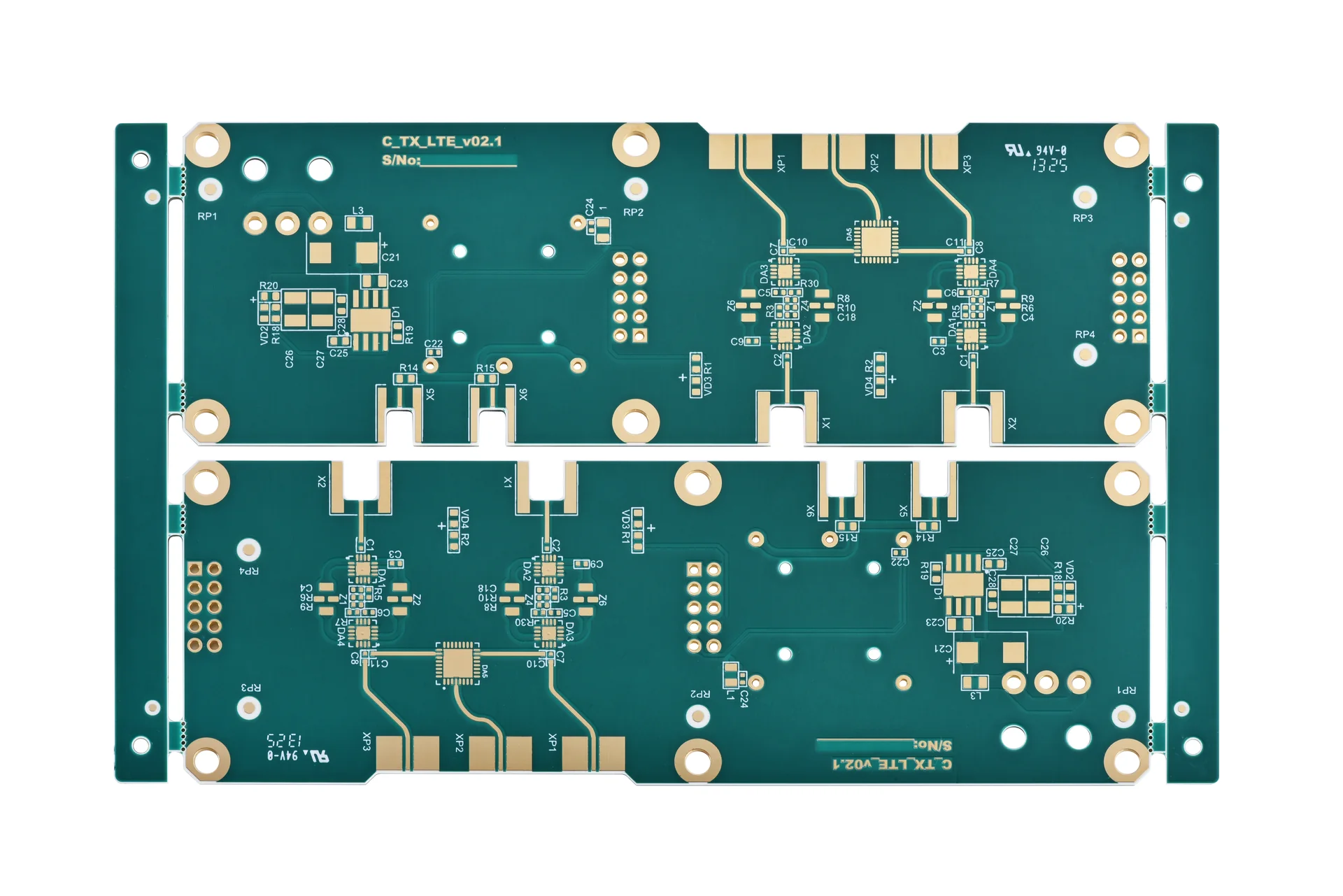
Traces and copper lands at the routed edge of a bare RF PCB.
Send the approved stackup with the connector drawing. A thickness change to satisfy the body fit can alter the reference spacing of the RF line, so it also belongs in the electrical review. Where a bracket, screw or other nearby feature locates the connector, include its mechanical relationship to the board outline and pad instead of dimensioning each from an unrelated reference.
For an illustrative fit check, suppose a connector drawing allows a local board thickness from 0.75 to 0.85 mm. A proposed board callout of 0.80 ± 0.08 mm spans 0.72 to 0.88 mm. The nominal value fits, while the allowed extremes extend beyond the connector range. Before release, review the thickness tolerance or choose compatible hardware and then recheck the launch geometry. Use the actual connector drawing to establish the limits for the order.
Drawing fields · Edge datum, routed profile, pad setback, local corner and breakaway conditions.
Show the finished edge on the copper and mechanical views. State the intended distance from that edge to the center land and ground features. Panel rails, tabs and other handling features should be reviewed against the seating region. If an edge tab leaves a residual nub at the launch, it can change how the connector body sits even when the overall board outline meets its nominal size.
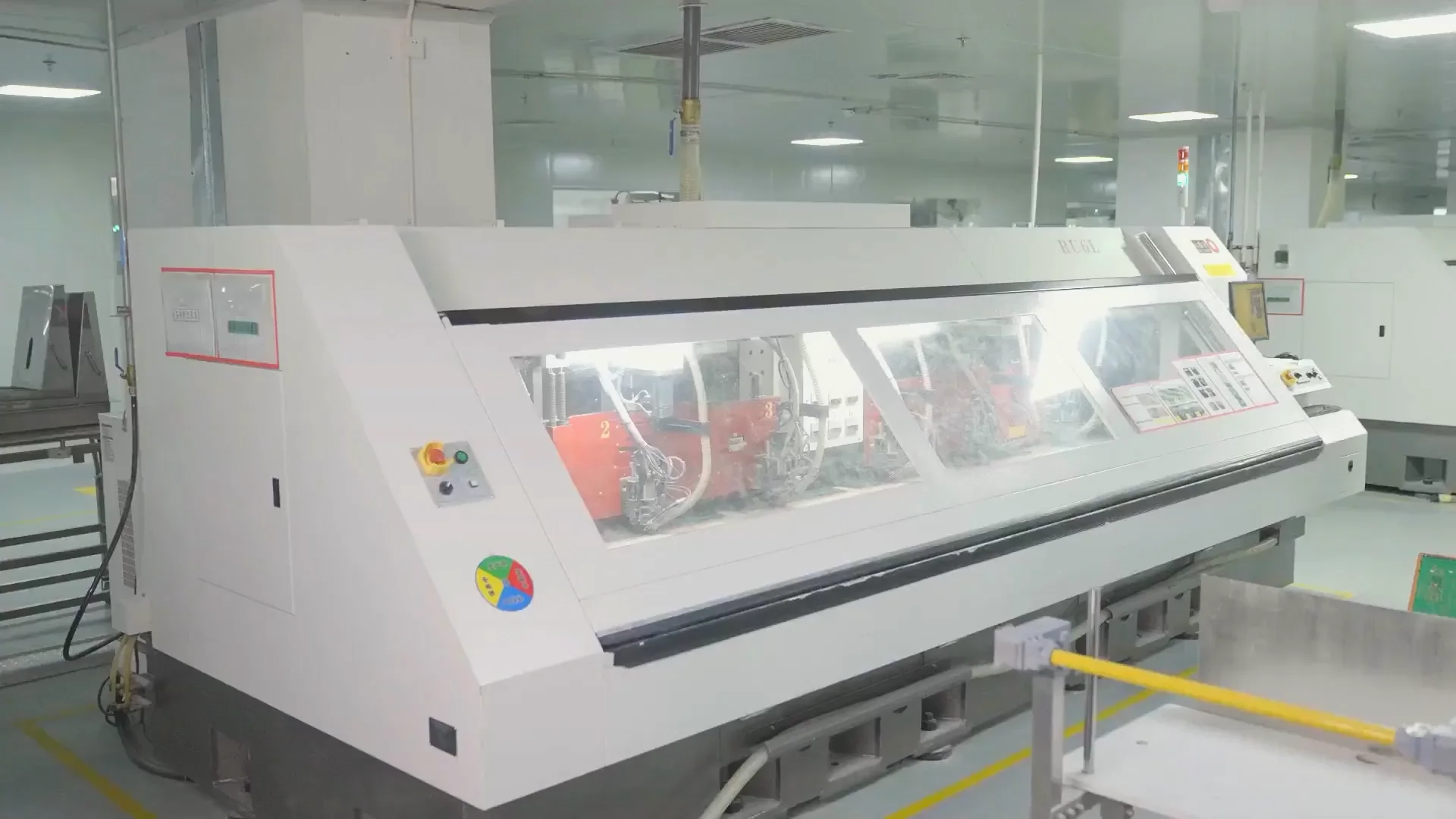
CNC equipment for forming PCB outlines.
Analog Devices’ edge-launch examples show that a gap between ground copper and the finished board edge can affect the return path and reflection. Where a design needs ground plating on part of the edge, define the plated segment, the layers it joins and the clearance around the signal. Agree the route and inspection for that feature with the fabricator before release.
Review the launch area on the same mechanical view that defines the routed edge. A line in a panel drawing may represent a process cut rather than the final seating face. If the location is critical, put a dimension and tolerance on the final unit detail, and identify which edge feature will serve as the inspection datum. Check how the team will handle an edge burr or residual tab in that region.
Drawing fields · Signal land, mask opening, ground pads, via connections, reference layers.
Place the center contact over the signal land in the mechanical view, then follow the signal into the first section of line. Compare land width, taper, coplanar gap and reference plane with the launch model or validated footprint for the chosen construction. If the connector body contacts ground on one or both faces, show those land positions and how the copper returns to the reference plane.
For a grounded coplanar line, rows of ground vias can join the top ground beside the line to the underlying reference plane. The grounded coplanar waveguide layout examples from Analog Devices illustrate that connection. Set via location and spacing for the actual launch, frequency and layer structure. Have the fabricator check the hole and pad clearances at the routed edge, where the routing and drill tolerances both affect the available space.
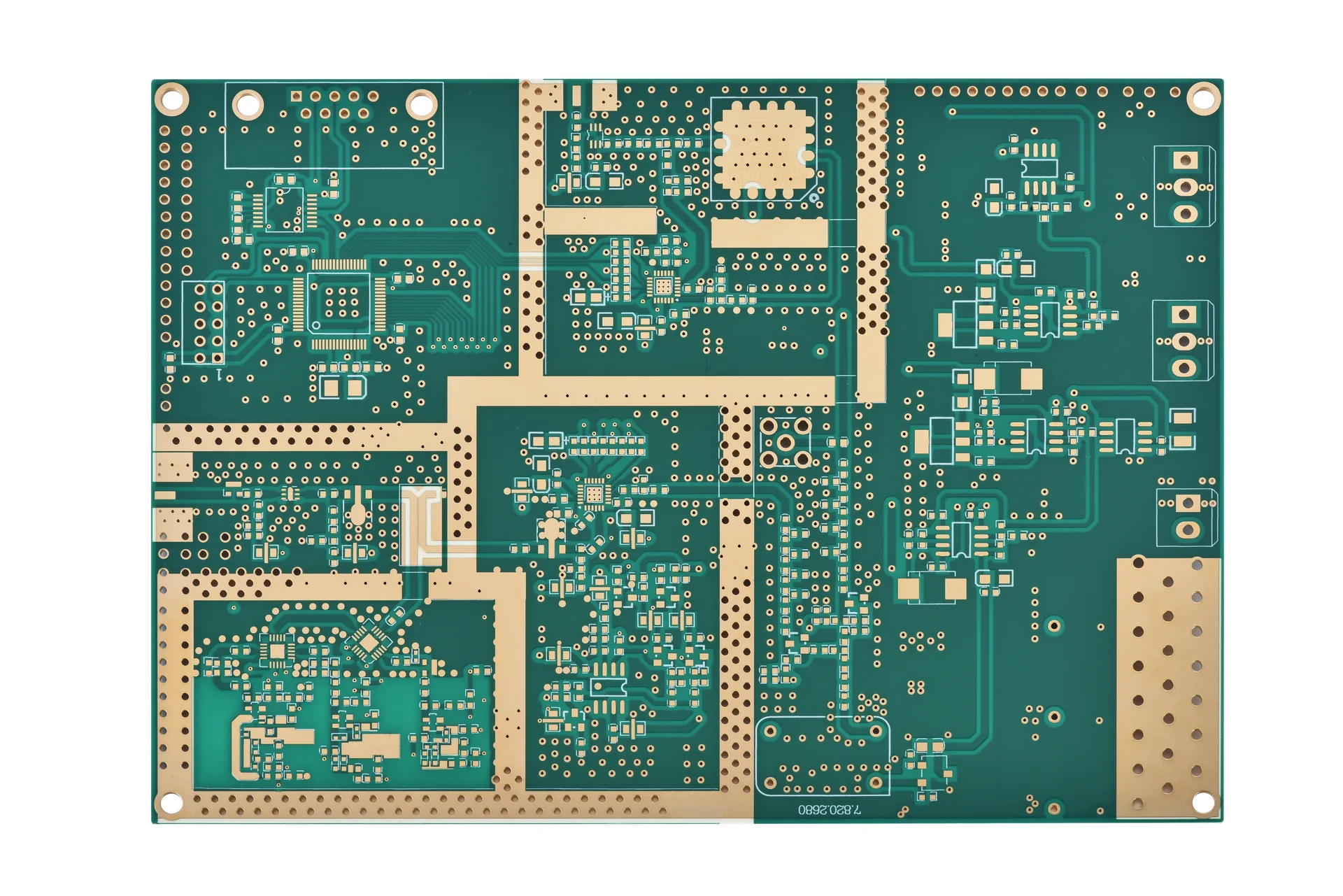
Plated-hole rows and surface copper features on a bare RF PCB.
Drawing fields · Revision, inspection dimensions, exception approval, electrical verification scope.
Include the connector drawing, local dimensioned detail, copper and mask layers, drill map and stackup in one revision. Record where to measure the finished thickness and pad setback. The controlled-impedance fabrication instructions cover the trace requirements. If a connector-mounted assembly also needs return-loss verification, define that test and its reference planes as a separate acceptance step.
For the first build, agree who will check bare-board dimensions and who will check the mating connector. If the electrical check includes the mounted launch, state the frequency range, test fixture and measurement reference. This gives the production team a clear distinction between a board dimensional result and the measured behavior of the assembled interface.
Example review request. Confirm the finished edge and local thickness against the selected connector drawing. Return any proposed changes to the pad, ground contact, via clearance or edge plating for engineering approval before tooling.
Send the launch detail and released files for high-frequency PCB fabrication review. If the final geometry depends on mating hardware or a fit sample, include that condition in the project request.
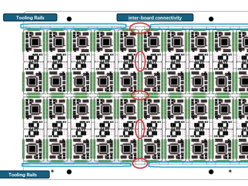
April/03/2026The Types of PCB Panelization
October/26/2026PCB Copper Thickness: Ounces, Microns and Resistance
September/01/2026LED Aluminum Core PCB Design to Manufacturing
November/03/2026HDI PCB Manufacturers in China: Comparison & 5 Key Checks
October/20/2026HDI PCB Manufacturer Evaluation: Prove the Build
Proven by 7 industries, 4000+ customer projects
Please contact us at sales@knownpcb.com, ask for engineering support here or use the form below to reach out to KnownPCB | Request a Manufacturing QuoteInclude your quantity, target delivery date and key requirements. File handling and NDA information. |