
In the PCB lamination process, a press bonds patterned cores, prepreg and outer copper into a single stack. The prepreg resin must flow into the spaces around the inner copper before it cures. The resulting dielectric thickness and layer positions affect both the board’s electrical geometry and where the drill can land on the internal pads.

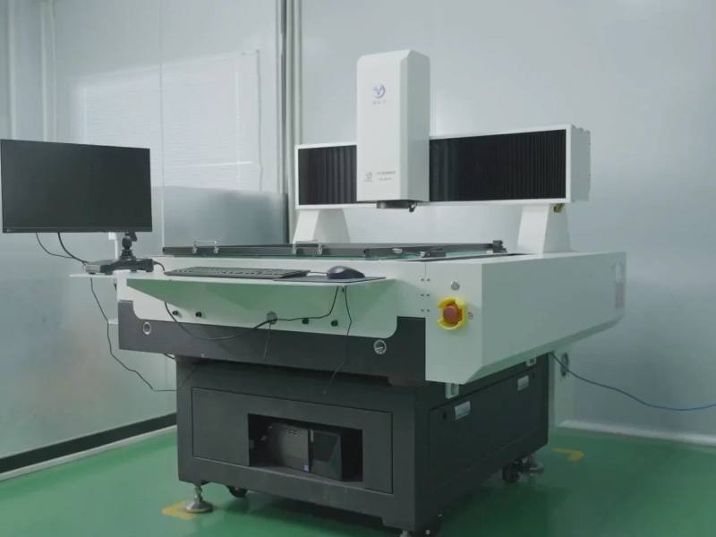
Copper-clad panels at an inner-layer preparation station.
Layup starts with the approved order of copper and dielectric layers. A patterned core supplies a cured dielectric with copper features on its faces. Prepreg supplies the resin-bearing reinforcement that bonds adjacent layers during the press cycle. Check the layer name, side and orientation on the actual production data. A correct material list alone cannot catch a reversed core or an artwork revision mismatch.
The copper pattern matters as much as the layer list. A region with large copper planes leaves different spaces to fill than a region with widely spaced traces. The material system, sheet selection and copper distribution all enter the estimate of cured dielectric thickness. In a controlled stack, use the pressed dielectric thickness between the relevant copper layers for the electrical calculation. A prepreg sheet’s nominal unpressed thickness is a material input. The target after lamination is a build requirement.
Before release — Reconcile the copper layers and their thickness definitions with the stackup. Identify the reference planes for impedance-controlled traces and record any material substitutions that require approval.
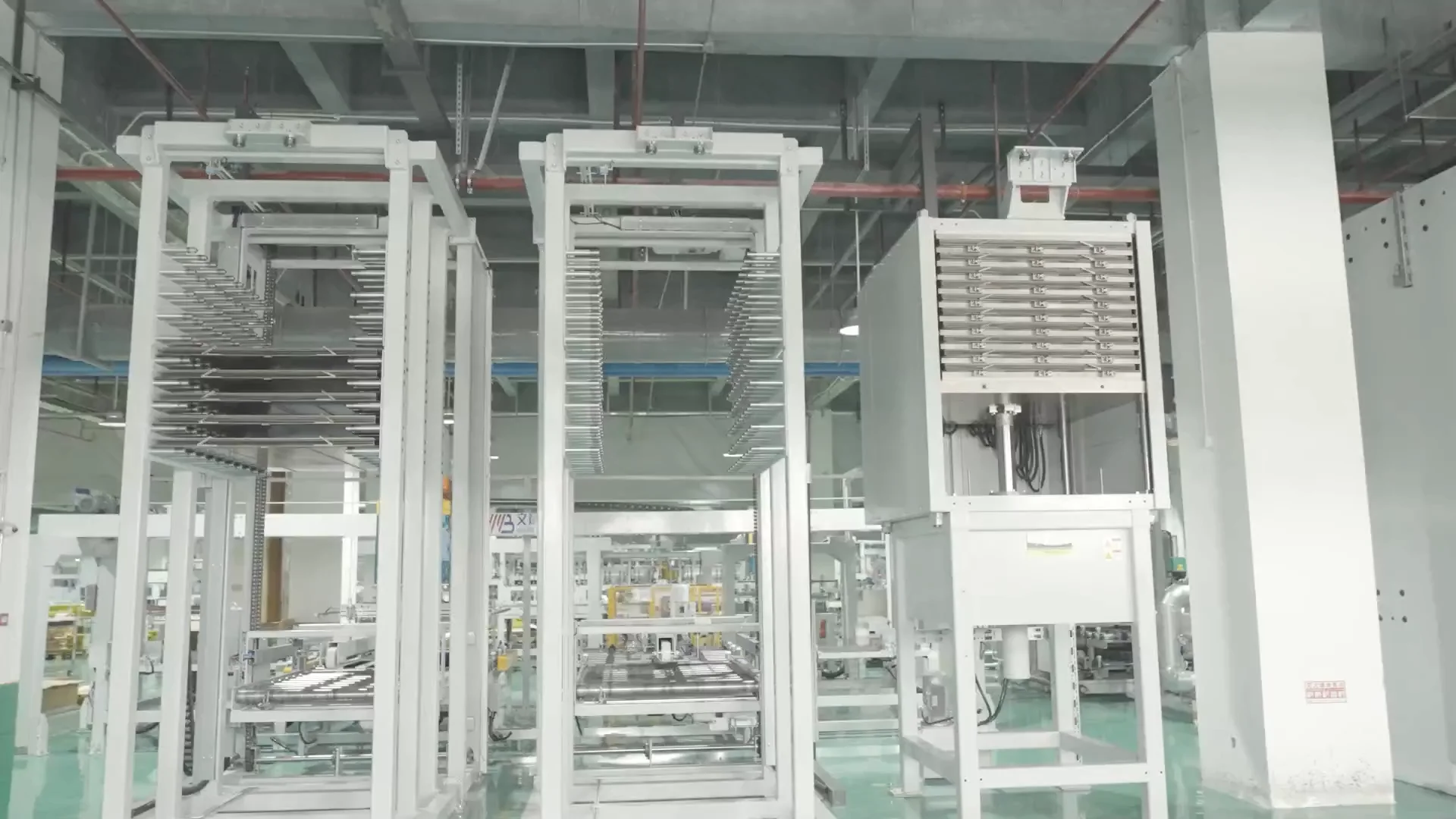
Lamination press equipment and panel handling racks.
The press cycle brings the stack through resin flow and cure under controlled conditions. As the resin heats, it can flow into the spaces beside the inner copper. The cycle must let the layers bond and reach the required cure. Pressing and flow can change the thickness of the resin-bearing layers, so the sum of the nominal sheet thicknesses does not establish the finished stack.
A production lamination schedule describes the pressure, temperature profile, cycle duration and cooling. These choices depend on the approved material system and build. With some vacuum-assisted layups, air removal helps control entrapped air. Separator plates and the way the layup is supported also matter when the board has a flatness or thickness constraint. The fabrication sequence described by Altium shows layup, press and controlled cooling as related stages.
During review — Ask the fabricator to confirm the actual material construction, the intended cured thickness for critical dielectric intervals and which regions need closer inspection. If a heavy copper region is close to a thin dielectric, show the copper distribution and the affected layers. A single board-thickness callout gives the total thickness, while a stackup detail identifies where spacing matters.

Panel handling after lamination.
The laminated panel now has internal copper that the drill must find. Lamination can change panel dimensions, and registration depends on the actual inner-layer pattern positions. In a route that uses internal targets and X-ray location, the measured targets can help establish the drill reference after pressing. The targets support alignment. They do not by themselves measure the remaining copper ring around every hole.
Keep thickness, alignment and adhesion findings separate. A section from an agreed location can show the local layer sequence, dielectric gaps and visible interface features. A thickness measurement at several defined locations answers a different question about the panel’s overall geometry. When a board has a tight annular ring, relate the inspection point to the layer and hole location described in the drill-to-copper inspection plan. If the observation is a separation or blister, check the location, the processing history and the applicable delamination investigation criteria.
Suppose two samples meet the total board thickness, but a section near a dense copper region shows a smaller gap between a signal and its reference plane. Report the affected interval and the section location so the team can compare like features. Changing the overall thickness requirement alone would leave that local spacing question unresolved.
After the press — Request the evidence that matches the design risk. State the layer pair and sample location for a dielectric measurement, the feature and plane for a registration check, and the conditions for any separate reliability test.
Start with a single approved stack drawing linked to the released board revision. Give the material identity, copper layer order and finished thickness. For each controlled dielectric interval, name the bounding copper layers and its thickness requirement. Where impedance is the governing requirement, give the trace layer, reference plane and target so the fabricator can reconcile the impedance review with the proposed construction.
Some HDI builds use additional lamination stages to make particular layer pairs accessible in sequence. In that case, show the drilled spans as part of the construction review. For a conventional multilayer build, concentrate on the actual layup, cured dimensions and panel alignment checks. Send the full build data for multilayer PCB engineering review when a material change, unusual copper distribution or close dielectric tolerance affects release.
October/06/2026PCB Plating Voids: Causes, Inspection and Prevention
April/09/2026Heavy Copper PCB Projects
September/28/2026PCB Desmear Process: Resin Smear Removal Before Hole Plating
October/28/2026PCB Z-Axis Expansion: CTE, Tg and Via Barrel Strain
April/23/2026Through-Hole Assembly Capabilities & DFM Checklist